

Their effects on its function may vary considerably, from brief tolerable faults such as short-time toggling of a port's output, for example, through to the IC's total failure, i.e. a permanent loss of function.
This article deals with conducted interference via IC pins. In these cases disturbances enter the IC via the electronic board's line networks. Electric and magnetic burst and ESD fields originating from the electronic board's environment are responsible for these conducted disturbances.
How do ESD and burst generate electromagnetic disturbances in an electronic system?
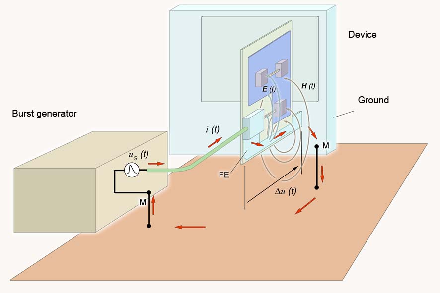
Disturbances that are injected in an electronic device during an EMC test produce magnetic and electric disturbance fields. These fields penetrate the electronic board (Figure 1).
Inductive coupling (B/H-field)
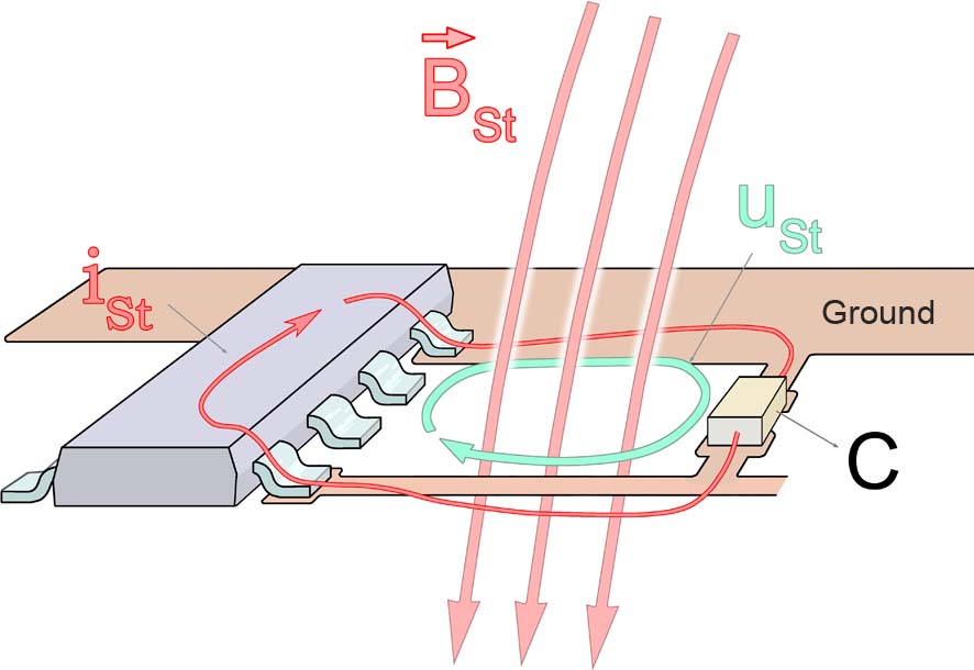
The lines of the electronic board form loops relative to the ground plane. If a magnetic field now enters these loops, a voltage to ground is induced in them. If the conductor loop is connected to an IC pin, the induced voltage to ground is present on this pin (Figure 2). The induced voltage may interfere with the useful signals on the signal line and drive a disturbance current into the IC.
Inductive coupling has a low source impedance and drives high-intensity currents into the IC. The current values are in the range up to 30 A. The line must be connected to ground outside the IC at a low resistance (capacitors) for the low source impedance to be effective.
Capacitive coupling (E-field)
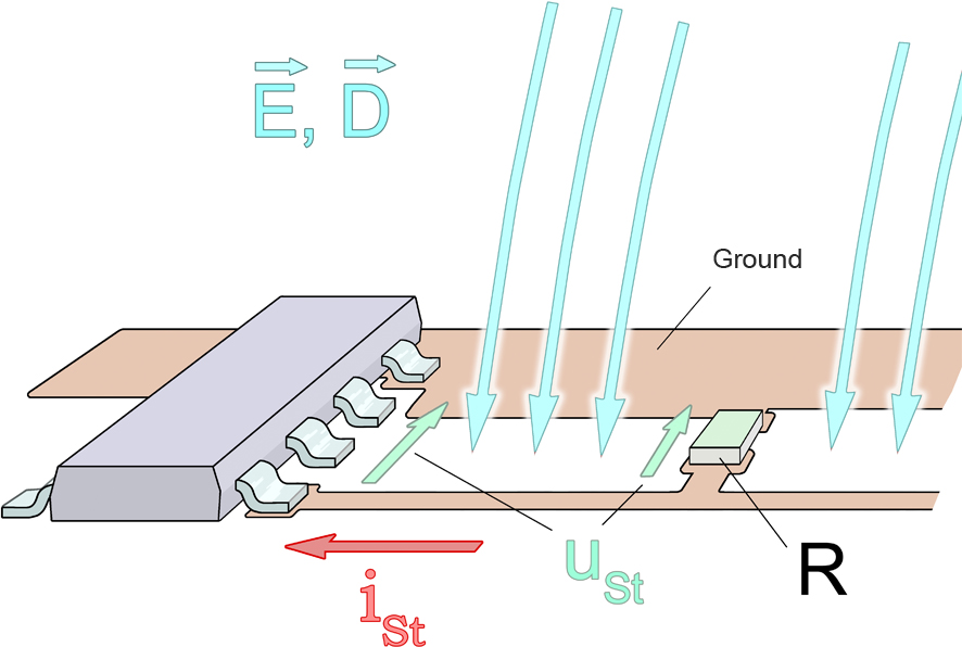
Lines on the electronic board form coupling electrodes for the electric field of the disturbance Figure 1. The electric field couples a disturbance current to the lines (coupling electrodes). The disturbance current flows to ground via a pull-up, pull-down or driver and generates a disturbance voltage drop across them (Figure 2). The induced disturbance voltage is present at the IC input and can modify useful signals or drive a disturbance current into the IC. Capacitive coupling has a high source impedance and drives low-intensity currents into the IC. The current intensity is in the range up to 1 A. The line must be connected to ground outside the IC via a pull-up, pull-down at a high resistance (resistor R) for the high source impedance to be effective.
IC pins with their EMC characteristics for conducted disturbances
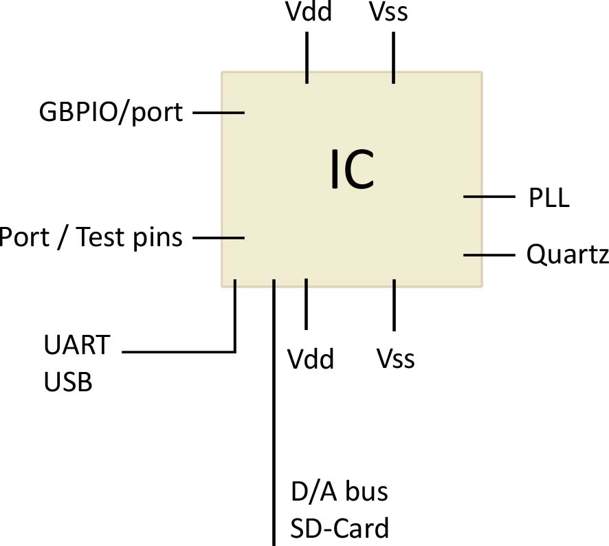
Conducted disturbances enter the IC via its pins due to capacitive or inductive coupling mechanisms. The characteristics of the coupling mechanisms together with the respective characteristics of the IC electronics connected to the IC pins are responsible for certain cause-and-effect relationships. IC pins can be classified in several pin groups depending on the EMC characteristics of the connected IC electronics.
The most significant groups of signal pins are:
- Port pins
- Test pins
- Interfaces (USB, UART, etc.)
- Bus pins
- Crystal oscillator connection pins
- Reset pins
- Supply pins: Vdd and Vss pins
Signal pins - Reaction of the IC to disturbances due to electric-field coupling
First possible reaction:
A disturbance voltage is superimposed over the useful signal as a result of capacitive coupling to the signal lines of the electronic board. The disturbance voltage changes the logic states of the useful signal. When the useful signal is read by the microcontroller, the following reactions are possible:
- The useful signal is checked for a possible disturbance by multiple scanning in the microcontroller. Spurious pulses can be filtered out based on this principle.
- If the test pin is not properly locked, a spurious signal switches the microcontroller over to the test mode, which in turn will result in the microcontroller's total failure.
- Interfaces have error detection and correction mechanisms that can detect and correct changes in the logic states of the useful signal.
- If the useful signal is a bus signal there is usually no protection against spurious pulses. The erroneous data, address or control signal is read and may lead to a microcontroller crash.
- Crystal oscillator connection pins
- Disturbances that are coupled to crystal oscillator connection pins may result in the failure of the crystal oscillator and the PLL circuit.1.
- If the useful signal is a reset signal, filters are arranged in the microcontroller to eliminate disturbances. The disturbance will be able to pass through the filters if these are not dimensioned adequately.
Second possible reaction:
The disturbance voltage that is coupled in rises up to the limit voltage of the protection diodes and opens them. A disturbance current thus flows into the IC's Vdd and Vss networks via the protective diodes. The disturbance current reverses the internal capacitances between Vdd and Vss. If a current flows in the negative direction, the internal capacitances will discharge and result in a supply voltage dip. This is not visible from outside. The microcontroller loses its logic register states and crashes. In addition, the disturbance current generates disturbance voltages across the series inductance of the Vdd, Vss system. These disturbance voltages cause interferences between different logic areas of the IC (chore, memory, PLL) and the resulting voltage differences interfere with the signal exchange between the logic areas.
The ESD protection diodes integrated in Vdd and Vss may also respond to this disturbance (power clamps) and short-circuit the IC if the circuitry layout is unfavourable. This may result in an IC failure or even its destruction.
Reaction of the IC to disturbances due to magnetic-field coupling:
A disturbance voltage is superimposed over the useful signal as a result of inductive coupling to the signal lines of the electronic board. Coupling is only effective if the signal lines on the electronic board are connected to ground at a low resistance. The best way to ensure this is to connect the signal lines to ground via a filter capacitor. The drivers' resistance is generally low enough to cause disturbances due to a magnetic field. These prerequisites allow the magnetic field to drive disturbance currents of a much higher intensity into the IC than the electric field. The effects are especially strong for power clamps. Depending on the inner impedance relations in the IC, the effect of the magnetic field can be weaker or stronger than that of the electric field. The two reactions described above for electric fields may also occur under the influence of magnetic fields.
Supply pins
Disturbances can usually only enter supply pins if a magnetic field couples to the supply networks of the electronic board.
The magnetic field drives a disturbance current into the Vdd / Vss loop of the IC. The disturbance current reverses the internal capacitances between Vdd and Vss. If a current flows in the negative direction, the internal capacitances will discharge and result in a supply voltage dip. This is not visible from outside. The microcontroller loses its logic register states and crashes. In addition, the disturbance current generates disturbance voltages across the series inductance of the Vdd, Vss system. These disturbance voltages cause interferences between different logic areas of the IC (chore, memory, PLL) and the resulting voltage differences interfere with the signal exchange between the logic areas. The disturbance effect is more intense compared to that of disturbance current entering the IC via the protection diodes due to an electric field. The disturbance current generated by the magnetic field can be up to 10-times higher than the current flowing via the protection diodes.
The disturbance current coupled to the Vdd/ Vss loop by the magnetic field can also cause the integrated ESD protection diodes to respond (power clamps). The IC may be short-circuited if the power clamp circuit has an unfavourable design. This may result in an IC failure or even its destruction.
Design rules for the IC environment – electric/magnetic-field coupling
The following design rules have proven successful to solve the aforementioned problems in practice.
Electric field
The effect of the electric field (ESD, burst) is attenuated or is prevented completely if the line networks of the electronic board to neighbouring ground areas are kept very short or are totally embedded in the ground plane. This means that the lines should be laid between two ground layers.
The IC pin's sensitivity determines the degree to which the line networks have to be shielded by ground. The IC pin sensitivity is a value that can be defined and thus also measured for each individual pin (Figure 5).
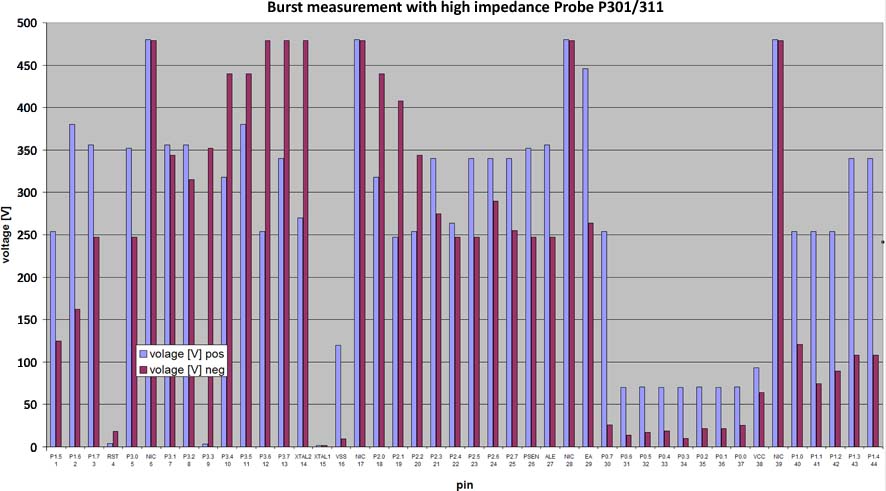
Figure 5 shows that the IC pin sensitivity varies considerably. If the pins are insensitive, line networks may lay at the surface of the electronic board unprotected by the ground plane without any disturbance due to an electric field (level of > 400 Volt in Figure 5). If the pins are sensitive, even complete shielding of the line networks by the ground plane may still be inadequate. The surface of a test point or the surface of the IC pin that is connected to the line network may be sufficient to absorb disturbance current from the electric field. The surface area of the line network (only a few square millimetres) is large enough to cause IC disturbances due to an electric field. The crystal oscillator connections of microcontrollers may have such a high sensitivity, for example (Figure 5 level of approx. 1-2 Volt)
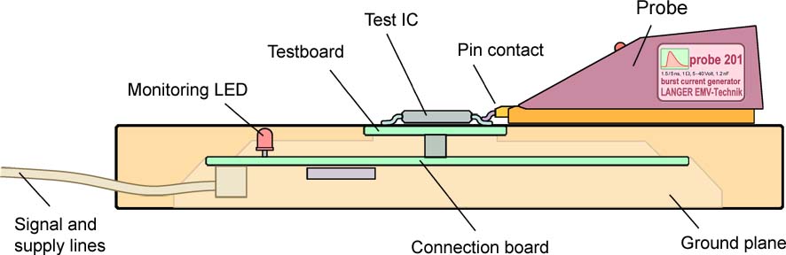
Figure 6 shows the measurement set-up to determine the sensitivity to conducted disturbances. The IC pins can be contacted separately with a special probe and a test pulse applied. This test pulse corresponds to the effect of the electric field (burst, ESD) on the line networks of the electronic board.
Magnetic field
The sensitivity of the IC pins to disturbance current pulses (burst, ESD magnetic field) can be shown in a diagram similar to Figure 5. The currents relevant for disturbances are in the range between 0.5 and 35 Ampere. If the pins are sensitive, induction loops of a few square millimetres are enough to cause inductive coupling. These loops may be formed by short line pieces with a layer distance of 0.5 mm to the ground plane. Blocking capacitors may also form critical loops, especially if arranged at the edge of the electronic board. The highest magnetic field intensity can usually be found there and this results in the highest voltage induction.
If the electronic board has a ground system with slots (separated ground), magnetic fields may enter and induce voltages in crossing line networks. This often happens if the analogue and digital ground planes are separated. The problem can only be solved if the ground planes are not separated and are continuously connected. The supply pins of crystal oscillator and PLL circuits are the most sensitive pins in practice. The IC's signal connections such as reset, crystal oscillator or test pins can also be very sensitive.
It is beneficial to match the layout design and mechanical structure to the IC pin sensitivity at an early stage of electronic board development. This increases the EMC immunity of the electronic board. Today, the conducted sensitivity of IC pins is already measured by the IC manufacturers.