

Today, strict cost minimization governs the development of electronic modules and pushes the development engineers for time. Measurements with a spectrum analyzer are often necessary in the course of product development. The engineers performing these measurements face a considerable workload as they have to precisely analyze and document the measured data. Comparing the spectra of pre- and post measurements, namely the frequency ranges of the measured near fields and subsequent changes to the module, is particularly time-consuming and a job that often has to be done in the sub-field of EMC emissions. The following article explains that the workload can be considerably reduced, measurements be made more efficient and time and costs be saved with software, taking practical EMI suppression measures as an example.
Compliance with high-frequency emission standards is tested in an EMC laboratory in the course of development. Should the emissions exceed any specified limits in far-field measurements, the electronic module has to be analyzed for the prominent interference frequencies and modified as required. This test and modification process may have to be performed in several cycles until the interference frequencies no longer exceed the limits specified in the standards.
Over the last ten years, the workload connected with the interference suppression process, and thus a lot of time and costs that would have been required for repeated tests in an EMC laboratory, could be considerably reduced mainly thanks to the development of near-field probes and small shielded cabins (shielding tents). Near-field probes allow the developers to measure local electric and magnetic fields on electronic modules at their workplace. The interference frequencies that occurred in the far field can thus also be analyzed in the near field and the components which are responsible for the interference emissions can be pinpointed. A shielding tent is a prerequisite for informative near-field measurements since it protects the measurement set-up from electromagnetic interference. Near-field measurements detect interference emissions that the module causes both directly and indirectly. The first example in this article deals with an emission analysis that uses near-field probes.
Another crucial time factor is the comparison and documentation of RF measurements during development. Major undesired emission effects occur when using capacitive touchscreens in particular. The second practical example in this article briefly describes how a capacitive touchscreen will work almost trouble-free and how certain standards relating to high-frequency interference emissions can be complied with. A simulated on-board power system is used in this context for emission tests in the course of development. The module has to be analyzed and improved if the interference emissions exceed the defined limits.
At first sight, a further reduction in the time and cost spent on interference suppression with near-field probes appears almost impossible. However, the development engineer's workload with regard to a quick and effective analysis of comparative measurements before and after modification of the module and their documentation has been ignored. Comparing series of measurements performed in connection with various modifications to modules, for example, is very time-consuming and costly since the spectrum analyzers used to measure interference frequencies usually only allow the export of an image of the spectrum displayed. Furthermore, the documentation of the image exports in a dedicated documentation program also causes a lot of work. These programs are used to document the exported images together with all measurement parameters and the respective descriptions which have to be transferred by hand. The problems described here as examples and further methodical weak points significantly reduce the efficiency of the development engineer's work.
Documentation of RF measurements with near-field probes
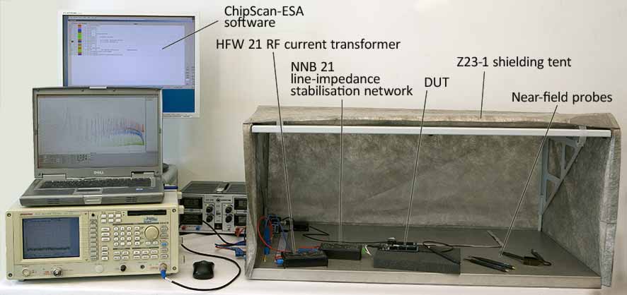
How the software works is described below on the basis of two examples. In the first example, a microcontroller board greatly exceeds the emission limits specified by the relevant standards during compliance measurements at an EMC laboratory. After returning to his workplace, it is now the development engineer's job to reduce the prominent interference frequencies. The components which cause the prominent frequencies of the emissions thus have to be localized on the one hand. On the other hand, efficient measures have to be found and used to reduce the interference frequencies. Finally, control measurements are performed to demonstrate the success of these measures. The microcontroller board is now placed in a set-up within a shielding tent that corresponds to its actual environment as far as possible so as to further analyze the precise origin of the interference frequencies (Figure 1). The shielding tent has an attenuation of approximately 50 dB and eliminates interference frequencies of other devices so that only the interference emissions from the microcontroller board are now examined. The supply lines such as power supply cables and cables to transmit the measurement results are led via the filters in the ground plane of the shielding tent. Since a large number of measurement and modification steps are required to suppress interference on the microcontroller board, the developer benefits from working consistently at his own workplace and from having direct and permanent access to the device under test, even during the measurements. The developer can thus make modifications directly to the device under test during a measurement. This allows him to examine changing interference emissions by simple manipulation (Figure 1).
In a first step, comparative measurements are carried out with a current transformer and the spectrum analyzer on the microcontroller board to verify the interference frequencies that occurred during the far-field measurement.
The initial state is usually recorded with several software products such as the recording software of the spectrum analyzer, a documentation software and possibly an image-processing software to process the recorded spectra. If only a few spectra have to be recorded, the workload connected with transferring the measurement data and the associated documentation within the individual programs by hand would perhaps be reasonable. However, several spectra quickly accumulate when analyzing a complex source of interference so that the workload connected with establishing a traceable documentation (log) may rise to several hours. Considering that measurements and documentation become necessary after each single modification, the workload increases even more.
The ChipScan-ESA software completely avoids all these transfers since it combines these three products, namely the recording software of the spectrum analyzer, documentation software and image-processing software, in one single software. The connected spectrum analyzer can be controlled directly and the spectra recorded with a mouse click. The necessary documentation text can be added to the recorded spectrum immediately. This allows the development engineer to record and document a large number of spectra simultaneously and directly, thus saving a lot of time.
Different near-field probes are used to narrow down and finally pinpoint the source of the interference frequency in the next measurement steps. The near-field probes are guided across the microcontroller board by hand for this purpose. They are swivelled and turned to determine the position and orientation of the interference fields. This information provides the developer with a pretty precise picture of the EMC situation on the microcontroller board. The measurements with near-field probes in different positions in our microcontroller board example show that the source of the interference frequencies is the microcontroller board itself. The responsible pin and core of the ribbon cable can be pinpointed precisely with the corresponding special near-field probes (Figure 2).
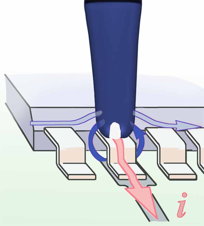
The internal clock signal is coupled out via one of the pins and the connected ribbon cable (Figure 3).
Text relating to the measurement on pin 13 from the measurement log: Pin 13 RF current in pin 13 measured with a RF-U 2.5 near-field probe, contains high shares of multiples of the processor clock rate in the range up to 300 MHz, cause for interference emission.
Text relating to the measurement on pin 12 from the measurement log: Pin 12 RF current in pin 12 measured with a RF-U 2.5 near-field probe, contains significantly fewer disturbances.
Possible measures that can be taken to suppress interference: the ribbon cable should be laid in a different position, at best within the inner layers of the circuit board of the microcontroller board where it is shielded at the same time. In addition, the ribbon cable should be kept as short as possible and, if it has to be laid outside, it should be located in the middle of the microcontroller board. The pin that is responsible for the emissions can be provided with a filter as another interference suppression measure. The RF filter was used to suppress interference on the microcontroller board on account of the small workload connected with this remedial action and the resulting low costs.
After implementing interference suppression, the measurement was repeated with the current transformer to exactly verify the benefit of the measure relative to its effectiveness in the respective frequency range. Should other interference frequencies exceed the limit value, their cause has again to be located with near-field probes and an appropriate solution to the problem found. Interference frequencies that were superimposed by the first emission source often become visible after this problem has been solved.
Comparing the individual measurement spectra by conventional methods is very time-consuming and expensive. Comparing hardcopies of the images exported from the spectrum analyzer by simply placing them alongside each other, for example, takes a lot of time and is rather prone to errors. This method does not allow the developer to exactly place the spectra on top of each other. Although this disadvantage can be overcome by printing the images on film, this would again push up the costs if a large number of spectra are involved. The images can be compared directly on the PC by means of an image-processing software and a semi-transparent representation of the spectra. However, this solution is time-consuming and cumbersome if several spectra have to be compared.
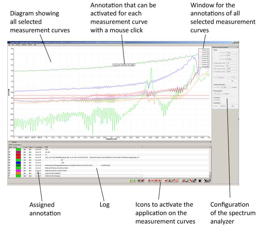
ChipScan-ESA can be used to directly compare any number of spectra in a single diagram in the wink of an eye (Figure 4). The user interface provides a clear overview thanks to the fact that individual spectra can be coloured, the annotation for an individual curve can be displayed and there is a separate window for all annotations in the diagram. ChipScan-ESA also allows the developer to compare the spectra of different overlapping frequency ranges and zoom in and out on them as he likes in the diagram view. The measured values can be shown exactly and read off if the mouse pointer is placed directly over the spectrum.
Documentation of RF measurements with a simulated on-board power system
The measurement on an on-board power system connection of a capacitive touchscreen is taken here as a second practical example. The use of capacitive touchscreens in products of the electronics industry leads to emission problems. Due to their mode of operation, capacitive touchscreens emit high-frequency electric fields into their environment. These high-frequency electric fields may interfere with other devices as a side effect. Limit value violations that are especially difficult to handle mainly occur in the frequency range between 150 kHz and 5 MHz during EMC measurements on the simulated on-board power system. Emissions are led into the vehicle via the cable harness if the capacitive touchscreen is connected to the on-board power system of an automobile.
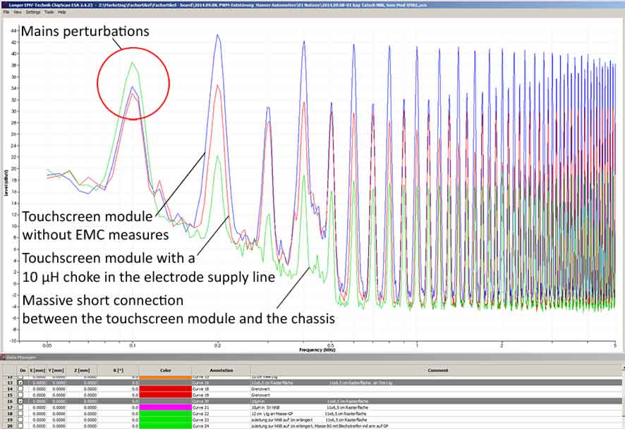
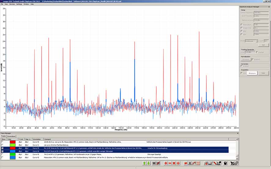
EMC countermeasures that are not described in this article were taken in the electronics and their effect was once again measured with a simulated on-board power system. Figure 5 shows the measurement results in the ChipScan-ESA software. The blue curve shows the module without any EMC countermeasures. The levels of the individual harmonics are highest here. EMC measures should reduce these levels. The red curve shows the effect of a 10 µH choke in the supply line of the electrode for a capacitive touchscreen. The level drops by approximately 10 dB. No change is noticeable for the fundamental frequency. This may be due to the fact that the 10 µH choke is dimensioned too small. Or there is a further EMC problem that has not been remedied by the choke.
The green curve shows the effect of a ground connection between the touchscreen module and the chassis, where this connection is designed as a wide and short connection. This measure results in a drop of > 20 dB in the harmonics. The thinner and longer the connection, the smaller its effect. A reduction of approximately 6 dB is achieved if the cross-section and length of the connection corresponds to the connection used to simulate the on-board power system.
The fundamental frequency of 100 kHz that is marked with a red circle does not originate solely from the electric field of the touchscreen electrode. It is also caused by system perturbations. The supply current of the RF voltage driver is not filtered sufficiently on its way to the on-board power system. The mains filter of the on-board power system connection of the touchscreen module is not dimensioned sufficiently.
Both examples clearly show that several series of measurements with a spectrum analyzer can be efficiently compared.
Additional functions of the measurement and documentation software
ChipScan-ESA offers additional mathematical operations (addition, smoothing, etc.) for further analyses of the spectra. For example, these operations allow the generation of envelope curves that can be used to analyze frequency limit violations. The current settings of the spectrum analyzer can also be stored and set in the spectrum analyzer if the measurement is continued at a later point in time. Furthermore, any type of diagram can be exported for presentation as image formats.
At the end of the emissions analysis, all spectra can be saved together with the associated documentation in a single file which then can be used for further future analyses.
The combination of all ChipScan-ESA functions enables a very easy and efficient analysis and documentation of interference emission problems or other RF measurements with a spectrum analyzer.