

Finding and Fixing Problems at the IC Level
Modern electronic device designs are increasingly small and complex, requiring more and more integrated circuits (IC). When a device’s ESD immunity is only first tested during the final development stage, detected problems are difficult, time-consuming, and expensive to solve. Thus testing a device, or better its individual components, during the initial design cycle is more efficient and can be done using a special test set-up to recreate the disturbance and the IC level. This article focuses on the impact of IC behavior on electronic design, specifically ESD characteristics and how they influence a device by influencing its ICs.
I. Influences on the IC in the Electronic
An IC’s susceptibility to fast pulse disturbances such as ESD, increases significantly when its structural dimensions, operating voltages, and operating thresholds are reduced. Developments in the ASIC- and microcontroller-design fields tend toward structures smaller than 100 nm. This in combination with higher switching rates results in a drop in disturbance immunity by around 90 percent – a drop also reflected by the device’s EMC behaviour.
Given identical functionality, an IC’s good EMC characteristics give manufacturers an edge over competitors. Thus it is the engineer’s objective to determine the parameters decisive for disturbance immunity and the electronic developer’s objective to use the most robust IC possible.
While ESD test standards at the device level have been available for years, no such regulations exist for a device’s individual parts (such as assemblies and components). Increasing complexity and, in particular, increasing component-integration density make it consistently more difficult to comply with device standards without having defined conditions at the IC level.
IC test pulses are defined on the basis of device test procedures. The respective test set-ups generate electric and magnetic fields within the device. These fields have a local effect on the interface of the IC package. IC test generators must be able to universally simulate the disturbances caused by these electric and magnetic fields. One existing method for individually testing an IC is the Human Body Model (HBM), though its ESD immunity results have no correlation to the device’s ESD behavior while in operation. Thus any protective mechanisms implemented to pass these tests are not viable solutions and may impact the device’s immunity negatively – even causing it to fail.
II. ESD Characteristics
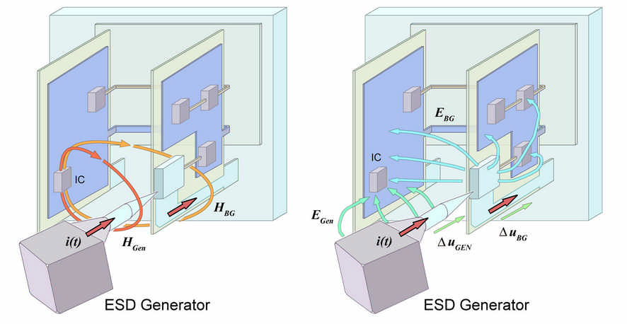
To understand in-test existent ESD interference one must be able to identify the interferences generated by the ESD gun used and analyze its unknowns (such as interference shape, etc.). While the current emitted via the tip of the ESD generator is described in the standard, it is distinct from the electric and magnetic fields emerging from both the object’s body and tip. The pulse shapes of these fields are different that the disturbance current and have an additional disturbance effect on the electronic device, possibly exceeding the desired effect. The extent to which these fields interfere with the electronic device is dependent on the positioning of the ESD generator in relation to the device’s modules. As the ESD generator is turned or tilted, weak points in the device may respond purely by chance making recognition and analysis of a device’s functional failures and their cause-and-effect relationship impossible.
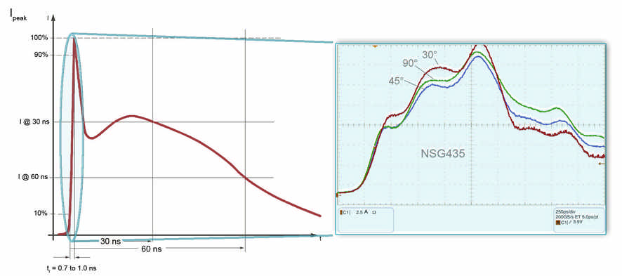
The typical ESD pulse shape as described in the standard 61000-4-2 (Figure 2) was measured using a test set-up and oscilloscope calibrated up to 4 GHz. Various unidentifiable deviations from the standard can be seen in the first peak. The rising edge of the ESD pulse is the most significant event because it has the fastest change in current and voltage, causing very strong electric and magnetic coupling. Also evident in the pulse shape are high-frequency transients with rise times up to 100 ps allowing for easier penetration of the electronic. Each of the three colors shown in Figure 2 represent a pulse shape based on a different angle and handling of the ESD generator during testing. While all fall within the scope of the standard, these variations prove the inaccuracy of any test results.
The effect is even more evident when oscillating the actual interference at an IC trace. When the ESD generator is contacted at one of the interface module’s shielded connectors and the disturbance current is coupled in, it is diverted and some of it flows through the GND-system to the electronic board where the IC is located and measurements on the traces are made. Even though the IC traces are not connected to the shielded connector, significant disturbances up to 70 V are measured at the IC input. These disturbances may, for instance, couple into the traces via the magnetic coupling inside the connector between the interface module and the electronic board. The ESD disturbance may couple into other traces because its current flows only into the shielding and GND systems. The board-to-board connector in the ESD disturbance’s discharge path also has impedance, causing a voltage drop between the two PCBs. The resulting electric field may also couple into the signal traces or into similar parts on the PCB. In Figure 2, the absence of any correlation between the resulting disturbance at the IC input and the actual ESD pulse shape is evident. Parts of the measured pulses are shorter than 200 ps.
III. Field influences at the IC
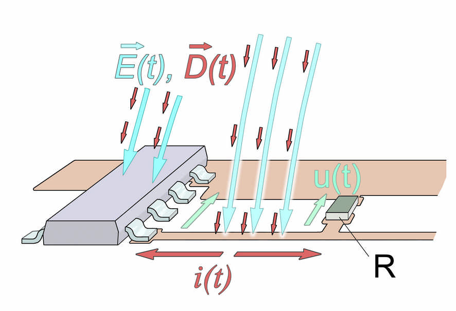
Lines with high impedance are mainly sensitive to electric interference. The voltage difference between the circuit and its environment (such as metal parts, ESD generator, and so on) generates an electric field that may affect the signals or the circuit. Such a difference in voltage may occur when, for instance, an ESD contact discharge is made on a nearby metal part. The disturbance current’s discharge path has impedance. Additionally there is a voltage drop between the metal part and the electronic, which will affect the electronic via the electric field. The resulting voltage pulse may disturb the traces or, depending on its sensitivity, the IC directly. This may be followed by signal corruption or the disturbance reaching other areas of the IC, through protection diodes for example, causing further problems.
Critical pins or lines include reset, clock, quartz, test pins, or high-impedance measurement inputs of A/D converters.
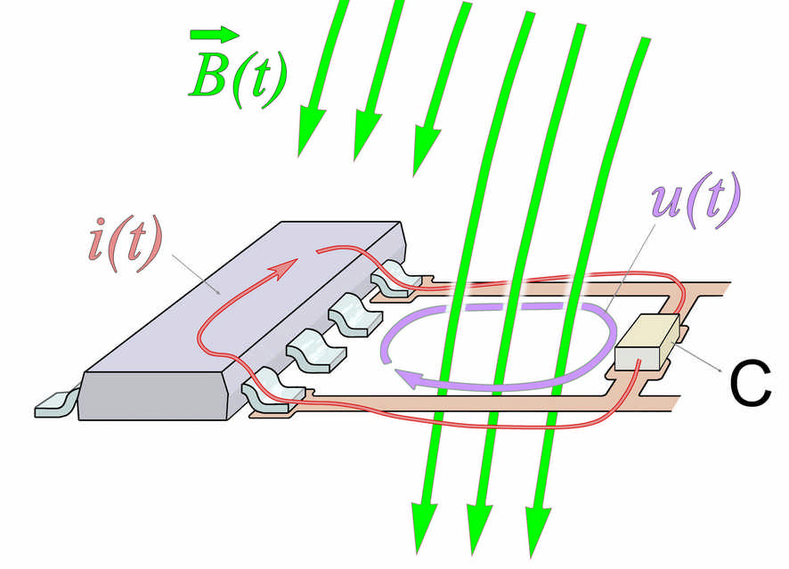
In the event of magnetic interference, the disturbance current generates a corresponding magnetic field in the device. This disturbance current may also occur as a result of a contact discharge at low-impedance connected metal parts. The derived current is always connected to the magnetic field and dependent on the construction of the set-up. This resulting magnetic field can induce a disturbance voltage in existing loops such as line networks on the PCB. This disturbance pulse drops at -- and therefore interferes with -- high-impedance IC inputs. Furthermore, the disturbance can also affect other areas within the IC such as the PLL, the core, and so on. Regarding magnetic-field interference, critical lines include the power supply system, low-impedance signals, and lines that are connected to GND or the power supply via a capacitor.
The electric field’s coupling mechanisms are determined by the capacitance between the IC’s line networks and its environment. The disturbance is derived when an IC input terminated with low impedance is subjected to capacitive interference. If the lines are connected at high impedance, the disturbance pulse is transmitted directly via the capacitive voltage divider. Ultimately, the effects on the IC are similar to those caused by magnetic coupling.
The magnetic field’s coupling effect can be compared to a transformer. Interference with the IC's low-impedance loops results in an inductive current divider. The disturbance current generated by the disturbance generator is transferred to the IC's line networks. IC inputs that are terminated with low impedance lead to the differentiation of the disturbance pulse caused by the magnetic field. The induced pulses have much faster rise times and are shorter than the actual disturbance generated by the ESD generator. Today's circuits are fast enough to evaluate and be affected by these derived disturbances, which can be much shorter than 1 ns.
To be useful, test procedures must simulate the field interferences in the device. A very low-impedance source, much lower than 50 Ohm, is required to simulate the disturbance coupling into the IC pin via the magnetic field. This allows a disturbance to be generated through voltage induction in the IC or at the line networks. A disturbance generator with a very high impedance, much higher than 50 Ohm, is required to simulate electric coupling. In conjunction with a very low coupling capacitance, this allows for the simulation of electric interference.
IV. IC test system
A test system developed by Langer EMV-Technik includes generators from the 200 and 300 series, which were designed according to the mechanisms used for coupling pulses into electronic assemblies and exactly simulating these physical interferences.
The effect mechanism of the magnetic field is characterized by the parameter of an external IC loop and the corresponding pulse magnetic field. In practical application these inductance loops can be created by traces capacitively shorted to GND (for example Vdd with bypassing capacitor). The voltage, with a peak value of roughly 40 volts, is induced in these loops. The generators in the 200 series were designed to share these characteristics. They consist of a pulse voltage source and a coupling network. The peak value of the pulse voltage source is adjustable and described as generator voltage, which is the amount of interference produced by the generator. The series connection of a resistor and inductor determine the current values. The probe is therefore constructed to have low resistance of about 1 Ω and a low inductance of about 2 nH. The internal capacitance ensures the galvanic separation from the GND. This allows the supply pins to be tested and the probe’s capacitor to act as a blocking capacitor.
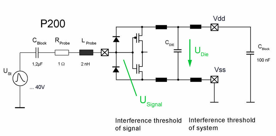
The 300 series generators, used to simulate disturbances caused by electric field pulses, couple a disturbance with a rise time around a nanosecond into the IC pin via an 18 pF coupling capacitor. The source’s internal resistance is 100 Ω and has an inductance of 50 nH – a relatively high impedance. The disturbance is shorted to Vdd/Vss in the IC via the protection diodes. The generator serves as a pulse current source. The current pulse is mainly determined by the generator’s internal parameters. The resulting maximum open circuit voltage is 500 V and corresponds to real conditions.
Using the Langer EMV-Technik IC test systems, the behavior of ICs can be investigated using targeted interference, regardless of whether they are field- or line-conducted or whether one is testing emission or immunity.
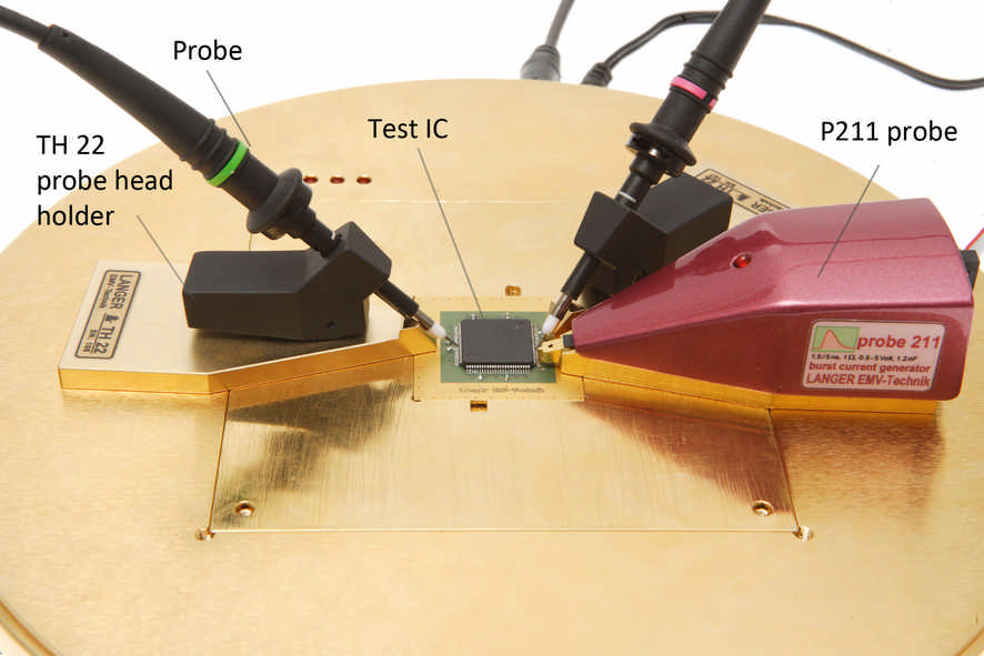
The IC is tested during standard operation. For this, the IC is removed from its application and placed onto a special IC test board. The test board is equipped with the DUT’s required circuitry as well as filters for all necessary supply voltages and signals to ensure functionality. The DUT’s high-frequency-compatible set-up is ensured by the massive metal plate which acts as reference GND and allows for measurements in a small area. The application is connected through a downward-led connector. Thus only the DUT is placed on top of the system and all other components are decoupled beneath the GND. These requirements are critical for measurements to be reproducible. The measuring system does not have to be integrated into the test board, but rather is located in the corresponding probes. The system was created for all IC measurements – standard or pre-compliant.
Some of the types of errors that can cause the controller to stop functioning include simple data errors, reset triggering, or hardware errors. Non-reversible errors such as a latch-up or defects in the internal oscillator circuit sometimes occur at high disturbance levels. Certain regions of the controller are more sensitive to disturbances. A cause of the error can be the controller’s core, which is located in this region. Measures that have to be taken by the user to make devices immune to disturbances depend on the design and function of the individual device. Susceptible lines have to be enclosed between GND layers, for example, to block electric or magnetic fields. These lines can also be protected by filter elements. The blocking capacitors near the supply pin reduce the size of the loop, where it may be possible to induce disturbance voltages.
Implementing this test system allows for a better and more complete understanding of the IC’s EMC behavior and through this knowledge the electronic developer is able to improve the EMC behavior of the entire device.