

Author: Stephan Pfennig
Published on: 13.03.2018
Motivation
If a device under test is affected during radiated immunity tests, appropriate countermeasures have to be taken depending on the interference level. In the case that the wave length of the test signal is large in comparison to the dimensions of the device, the interference quantity typically couples onto larger structures, e.g., onto the device's cables. Subsequently, the interference can couple galvanically, inductively or capacitively into individual areas or single components of the device. An integrated circuit (IC) could be such a component. To select the appropriate countermeasures, it is very helpful if the coupling paths and coupling mechanisms can be identified.
For measuring the inductive and capacitive coupling into ICs, the Langer EMV Technik GmbH developed a method for measuring the immunity separately for the electric and magnetic field. This method was presented in [1] and was used in [2] to investigate the shielding effectiveness at IC level using different shielding configurations and materials. Thereby, it was distinguished between the shielding effectiveness for the electric and magnetic field.
Measurement Set-up and Shielding Configurations
To investigate the shielding effectiveness, the IC Test Environment ICE1 and the IC Test System P1402/P15021 were used. For the measurement set-up, the ground plane GND 25, the accompanying adapter GNDA 02, the field probes EPM 02 and BPM 02 for measuring the electric or magnetic field, the ring-shaped spacer D70 h10 with a height of h = 10 mm, the field source P1402 for creating a magnetic test field and the field source P1502 for creating the electric test field, were used. Additionally, the pre‑amplifier PA 303 was used. The individual components and the measurement set-up are shown in Fig. 1.
---------
1 IC Test Systems P1401/P1501 and P1402/P1502 for inductive and capacitive coupling into ICs up to 1 GHz or 3 GHz
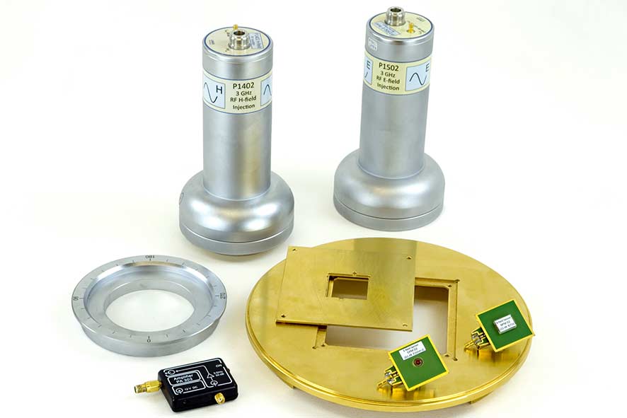
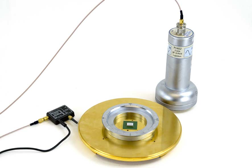
For the measurement, the respective field probe was placed into the ground plane instead of the IC and the respective field source was placed onto the ground plane (above the field probe) using the ring-shaped spacer. Finally, the network analyser’s (NWA) output was connected to the field source, the field probe was connected to the pre‑amplifier and the amplified signal was returned to the network analyser’s input. Before the measurements, the NWA was calibrated to the input of the field source and the output of the pre‑amplifier.
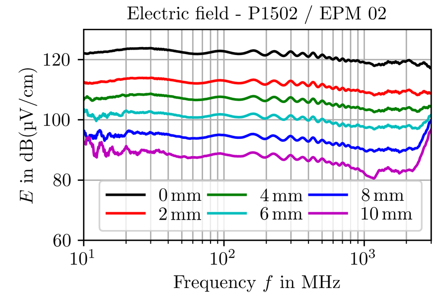
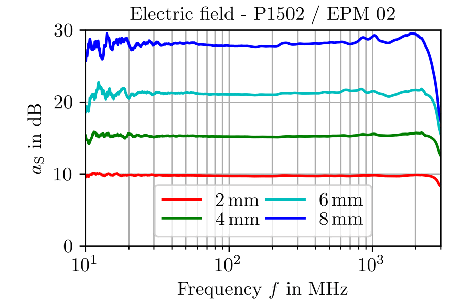
Based on the described set-up, the systems insertion loss (forward-transmission factor S21) was measured with and without the shield. Using the field probes conversion factors and the pre‑amplifier's gain, the electric field strength and magnetic flux density were calculated from the measured data. Finally, the shielding attenuation as was calculated for the electric and magnetic field.
To investigate the shielding effectiveness, different shielding configurations were used. For the investigation, a piece of filling material—a dummy IC made from Styrodur—was placed on the field probe. Finally, the respective shield was applied to the dummy IC.
Theoretically, the most effective shielding is obtained for a shield, which fully covers the IC and is connected to ground all around the IC. Practically, this cannot always be implemented or is not an appropriate measure for financial reasons.
For a first, simple approach, strips of self-adhesive copper tape were used. For the measurements, the width of the strips was varied. It was distinguished between the shield being connected to ground at one side or at both sides. [2]
Results for Copper Tape and the Strips Connected to Ground at Both Sides
As a first step, the shielding effectiveness was measured for self-adhesive copper tape using strips with a width of b = (2,4,6,8,10) mm. The results for the shielding of the electric and magnetic field are given in Fig. 2 for strips connected to ground at both sides. In general, the results show that the shielding effectiveness improves with the width of the strips.
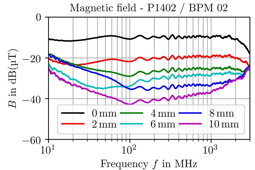
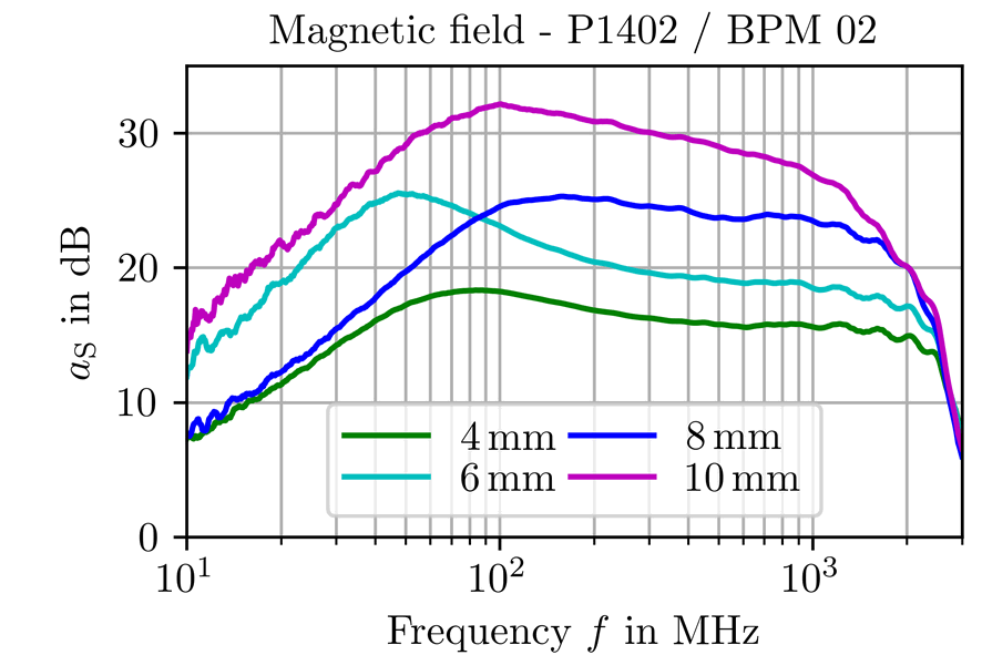
The results for the electric field show that the shielding attenuation is approximately constant in the frequency range up to 2 GHz. For the magnetic field, the shielding attenuation is relatively small for low frequencies, but increases with approximately 20 dB per decade. In the upper frequency range, the shielding attenuation is approximately constant up to 2 GHz.
If the strips are connected to ground at both sides, the shield creates a short circuit loop. The mechanism of a short circuit loop for shielding magnetic fields is explained in [2] using the example of shielded ICs. There, it is shown that the results agree well with the analytically derived behaviour.
The observed shift of the curves in the lower frequency range can be also explained with the equations derived in [2]. This shift is caused by the ground connection which depends on how well the shield is applied to ground and, therefore, yields a varying contact resistance between the copper tape and ground [2].
In the case of a poorly connected shield and a correspondingly large contact resistance, the shielding attenuation for magnetic fields is reduced significantly, especially in the lower frequency range.
Results for Copper Tape and the Strips Connected to Ground at One Side
The results for connecting the shield only at one side are given in Fig. 3. The results for the electric field show that the shielding effectiveness is not affected in the lower frequency range. The displacement current created by the electric field flows to the shield and over the one-sided connection to ground. In the upper frequency range, the behaviour changes due to the capacitance between the shield and ground taking effect. The capacitance and the self‑inductance of the strip create a LC resonator. As both, the capacitance and the inductance, depend on the width of the strip, the resonant frequency shifts accordingly.
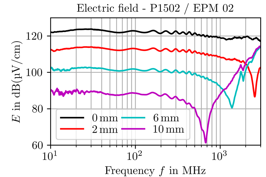
Considering a shield which is only connected to ground at one side, the capacitance and the inductance are relatively large if a wide shield is placed directly above the IC and if this shield is only connected to ground over a narrow connection. In that case, the resonant frequency is relatively small. As the shielding attenuation decreases significantly above the resonant frequency, the shield should at least be connected to ground as wide as possible if the shield is only connected at one side.
The results for the magnetic field show that there is no shielding effect if the shield is only connected at one side to ground and, therefore, no short circuit loop is created.
Comparison between Copper Tape and a Shielding Tape
In [2], the shielding effectiveness of the self‑adhesive copper tape and a self‑adhesive shielding tape2 is compared. For the comparison of the two shielding materials, strips of the same width were applied to the dummy IC and connected to ground at both sides. The results for the shielding of the electric and magnetic field are presented in Fig. 4.
---------
2 Self‑adhesive tape based on the braided and aluminium‑coated fleece LBVM1‑S5 manufactured by Schirmung 2000
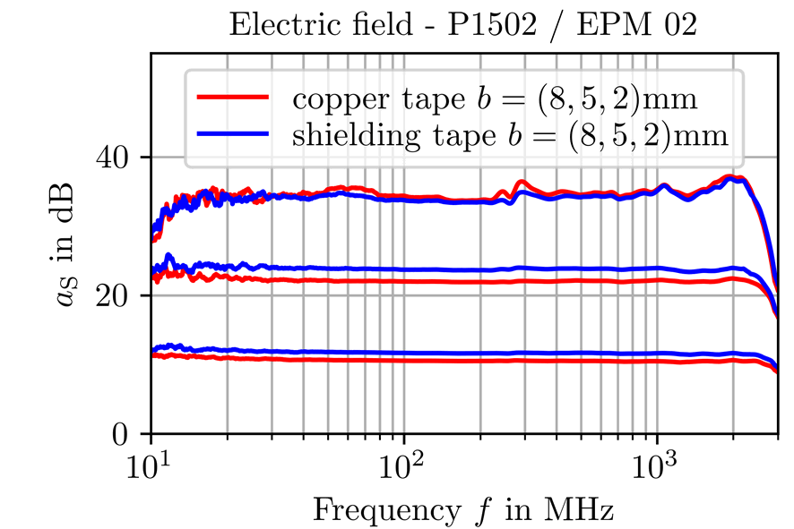
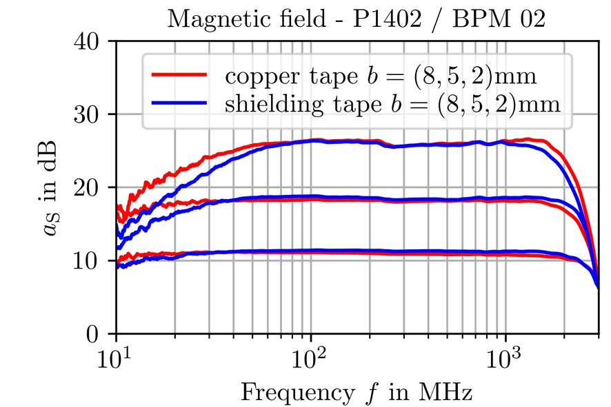
If the connection to ground is carried out well and, therefore, the contact resistance between shield and ground is small, the two materials yield approximately the same shielding performance.
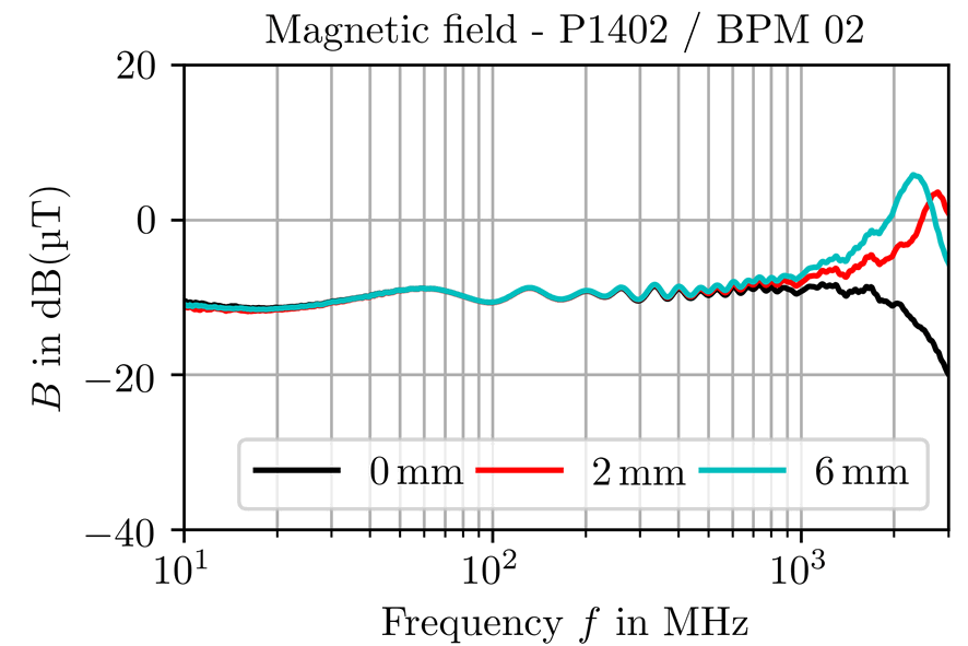
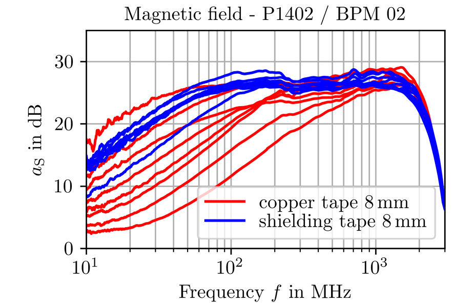
But the results presented in [2] also show that the shielding attenuation of the self-adhesive copper tape can, depending on the contact resistance, vary significantly, especially in the lower frequency range. A first impression is given by the results in Fig. 5 obtained for shielding strips with a width of b = 8 mm.
Literature
| [1] | PFENNIG, Stephan ; LANGER, Gunter: Messung der Störfestigkeit integrierter Schaltungen getrennt für das elektrische und magnetische Feld. In: emv - Internationale Fachmesse und Kongress für Elektromagnetische Verträglichkeit, 2018 |
| [2] | PFENNIG, Stephan: Measuring Shielding Effectiveness at the IC Level. In: 2017 IEEE International Symposium on Electromagnetic Compatibility & Signal/Power Integrity (EMCSI). http://dx.doi.org/10.1109/ISEMC.2017.8078011 | DOI: 10.1109/ISEMC.2017.8078011 |