

Author: Stephan Pfennig
Published: 25.07.2018
1 Motivation
Development-related testing of the electromagnetic compatibility (EMC) is an essential part when developing electronic devices and systems. In this context, the properties of the electronic components themselves gain more importance, for example the electromagnetic compatibility of the integrated circuits (ICs).
With regards to the compatibility of entire devices or systems, it is advisable to use ICs with high level of immunity and low level of emissions. In particular cases this can be decisive whether a device meets the requirements for its electromagnetic compatibility. A practical example are devices, whose housings do not have an electrically conductive surface and therefore do not have shielding properties. In that case, interference quantities from the environment can, to a greater extent, couple into the device and therefore lead to electromagnetic interferences. Accordingly, interference quantities generated within the device can, to a greater extent, couple to the environment.
To ensure the electromagnetic compatibility in general, or in particular, devices without shielded housings, the circuit as well as the circuit layout have to be optimized. This can include to only use ICs, which meet the requirements regarding their immunity and emissions.
In order to evaluate and compare integrated circuits, the Langer EMV-Technik GmbH developed different IC test systems. In the following article, those systems will be presented including an allocation to the currently existing, standardized testing and measurement techniques.
2 Overview of Current Standards
For testing the electromagnetic compatibility of integrated circuits, different standards exist. The testing of electromagnetic emissions is specified in IEC 61967 and the testing of electromagnetic immunity in IEC 62132. The immunity to transients is considered separately in IEC 62215. This standard, for example, refers to the test pulses defined in IEC 61000‑4‑4 and IEC 61000‑4‑5 (burst, surge). An overview of selected testing methods, specified in the above-mentioned standards, is given in Table 1.
| Electromagnetic Compatibility - Testing and Measurement Techniques | |
|---|---|
| IEC EN 61000-4-2 | Electrostatic discharge immunity test (ESD) |
| IEC EN 61000-4-4 | Electrical fast transient / burst immunity test |
| IEC EN 61000-4-5 | Surge immunity test |
| Integrated Circuits - Measurement of Emissions | |
|---|---|
| IEC 61067-2 | TEM cell method |
| IEC TS 61967-3 | Surface scan method |
| IEC 61967-4 | 1 Ω/150 Ω direct coupling method |
| IEC 61967-8 | IC stripline method |
| Integrated Circuits - Measurement of Immunity | |
|---|---|
| IEC 62132-2 | TEM cell method |
| IEC 62132-3 | Bulk current injection method (BCI) |
| IEC 62132-4 | Direct RF power injection method (DPI) |
| IEC 62132-8 | IC stripline method |
| IEC 62132-9 | Surface scan method |
| Integrated Circuits - Measurement of Pulse Immunity | |
| IEC TS 62215-2 | Synchronous transient injection method |
| IEC 62215-3 | Non-synchronous transient injection method |
| Table 1: Overview of selected methods for testing the electromagnetic compatibility of integrated circuits | |
3 IC Testing Systems
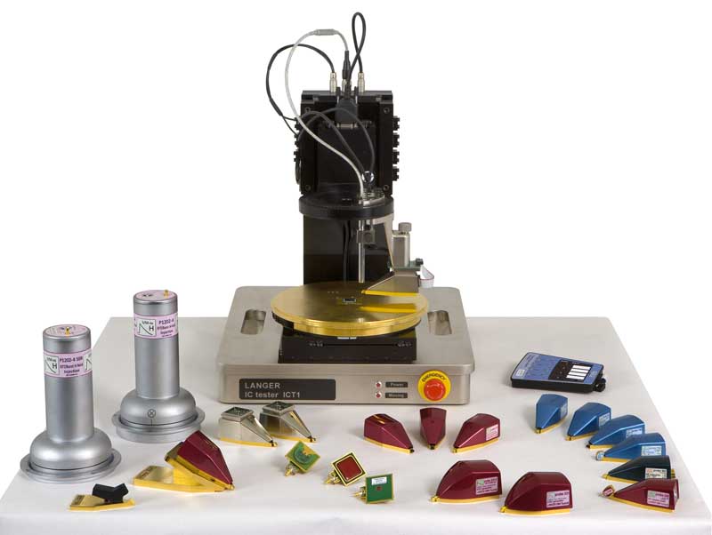
For measuring the immunity and emissions of ICs, the Langer EMV‑Technik GmbH developed different testing systems. Those are particularly suitable for evaluating and comparing the properties of ICs. An overview of the currently available testing systems is given in Table 2.
In general, the IC testing systems offer the advantage, that the interferences or, respectively, the error patterns that are caused by the susceptibility of the IC and that are normally observed first during the EMC test of the device or system, can already be identified during the IC’s EMC tests. That means, appropriate counter-measures can already be taken at IC level. Furthermore, if the EMC related properties of ICs are available, respective ICs can be selected depending on the requirements given for the application.
As shown in Table 2, the IC testing systems can be assigned to three areas - systems for measuring the immunity to transients, systems for measuring the immunity to RF and systems for measuring the emissions. For all three applications, it can be distinguished between conducted (or direct) coupling and field coupling in the near field of the ICs.
| Measuring the Immunity to Transients | |
|---|---|
| conducted coupling | field coupling (near field) |
| → IEC 62215-3 P250 set (Burst, IEC 61000-4-4) P331-2 set (ESD, IEC 61000-4-2) P331 set (EFT, τr = 0.2 ns) P202/P302 set (EFT) | P1202-4/P1302-4 set (Burst) P1202-2 set (ESD) P1202/P1301 set (τr = 0.2 ns) |
| Measuring the Immunity to RF | |
|---|---|
| conducted coupling | field coupling (near field) |
| → IEC 62132-4 P501/P503 set P512 set | → alternatively to IEC 61967-2/-8 P1401/P1501 set (1 GHz) P1402/P1503 set (3 GHz) |
| Measuring the Emissions | |
|---|---|
| conducted coupling | field coupling (near field) |
| → IEC 61967-4 P603-1/P750 set (1 Ω/150 Ω) S603/S750 set (1 Ω/150 Ω) | → alternatively to IEC 61967-2/-8 P1601/P1702 set (1 GHz) P1602/P1702 set (3 GHz) |
| → IEC 61967-3 ICR sets (near-field micro probes) | |
| MFA sets (active near-field micro probes) | |
| Table 2: IC testing systems for measuring immunity and emissions | |
| IC Security | |
|---|---|
| fault injection | side-channel analysis |
| ICI 03 L-EFT set + ICS 105 set (1 Ω/150 Ω) ICI-DP sets + ICS 105 set (1 Ω/150 Ω) | ICR sets (near-field micro probes) + ICS 105 set |
In general, for field coupling it is distinguished between radiated field coupling and near-field coupling. Additionally, for near-field coupling it is distinguished between electric-field (capacitive) coupling and magnetic-field (inductive) coupling.
For the testing systems listed in Table 2 under near-field coupling, the distance between the IC and field source or the IC and the field probe is so small, that—for the frequency range considered—the IC is located in the near field of the field source (immunity) or the field probe is located in the near field of the IC (emissions).
3.1 Immunity to Transient Interferences
A test method for injecting non-synchronous transients (pulses) is specified in IEC 62215‑3. The injection is referred to as non-synchronous, because the injection of the test pulses is not synchronised to the IC’s internal system cycle. The standard specifies, that ICs used for industrial applications, have to be tested to typical transients, as for example defined in IEC 61000‑4‑4 (burst) and IEC 61000‑4‑5 (surge).
For this purpose, the Langer EMV‑Technik GmbH developed different IC testing systems that generate the respective transients (EFT1) and that are suitable for reproducibly testing the IC’s immunity.
The IC Test System P250 set is used to test the IC’s immunity according to IEC 62215‑3 to burst. Using a standard-compliant burst generator (IEC 61000‑4‑4) the test pulses are generated and coupled capacitively to the respective pins using the coupling network P250.
Transients, as resulting from electrostatic discharges, can be generated with the IC Test System P331 set and P331‑2 set. Using the P331‑2 set, test pulses, as defined in IEC 61000‑4‑2, are generated and coupled directly into the tested pin of the IC. Using the P331 set, test pulses with a smaller rise time (τr = 0.2 ns) are generated [1]. Due to the smaller rise time, this test is more stringent compared to the standard-compliant pulse (τr = 1 ns).
The IC Test System P202/P302 set can also be used for testing the immunity to transients by coupling the test pulses directly into the respective pins. The system includes two generators, P202 and P302, as well as a pulse current probe and a pulse voltage probe. The generated test pulses are derived from the different coupling mechanisms and emulate typical disturbance pulses observed at the inputs of ICs when exposing a device or system [2].
With the IC Test Systems P1202‑4/P1302‑4 set, P1202‑2 set and P1202/P1301 set the same test pulses—mentioned above—can also be coupled inductively and capacitively to the IC under test. That means, the IC is exposed to the resulting electric and magnetic fields, as for example created when exposing a device or system to electrostatic discharges.
The IC Test System ICI 03 L‑EFT set creates fast transients and was especially developed for performing side-channel analysis. With the three sources included in the system, the generated test pulses can be coupled capacitively (electrically), inductively (magnetically) or directly over a contact tip (forward body biased injection) to the IC.
1 electric fast transient
3.2 Immunity to Continuous Interferences
For integrated circuits, measuring the immunity to conducted and radiated interferences is specified in IEC 62132. A method for direct power injection is described in IEC 62132‑4. For measuring the radiated immunity a TEM cell (IEC 62132‑2) and a stripline (IEC 62132‑8) can be used. For the direct RF power injection, the IC Test System P500 set can be used. The P501 and P503 contain a measurement system for detecting the current and voltage of the injected power. The P512 enables power injection into pins at frequencies up to 12 GHz. The coupling network used is fed by an external RF signal generator and power amplifier, and couples the test signal directly to the IC’s pin under test.
The IC Test Systems P1401/P1501 set and P1402/P1502 set are specially developed for measuring the immunity of ICs separately for the electric and magnetic field. The field sources P1401 and P1501 or the field sources P1402 and P1502, respectively, create an electric or magnetic field, which is used for testing the IC’s immunity in the near field of the respective field source. This method was presented in [3] and can be used for frequencies up to 1 GHz or 3 GHz. The separate testing of the IC’s immunity to electric and magnetic fields is particularly suitable for development-related testing and can be used supplementary to the testing in a TEM cell or IC stripline.
3.3 Emissions
IEC 61967‑4 describes a method for measuring the conducted emissions, which is referred to as 1 ohm/150 ohm direct coupling method. For measuring the respective interference quantity—the interference current or voltage—an RF probe with a 1 ohm-shunt or an impedance matching network with an input impedance of 150 ohm is used. For this method, the IC Test System P603‑1/P750 set was developed. The system contains the RF probe P603‑1 and the matching network P750. For the measurement, the RF probe’s contact tip or the matching network’s contact tip, respectively, is connected directly to the respective pin of the IC. Alternatively, the IC Test System S603/S750 set can be used to measure the conducted emissions. In comparison to the P603‑1/P750 set, the RF probe S603 and the impedance matching network S750 are connected to the test board via SMA-connectors.
For measuring the radiated emissions up to 1 GHz or 3 GHz, respectively, the IC Test Systems P1601/P1701 set and P1602/P1702 set were developed. Using the field probes P1601 and P1702 or P1602 and P1702, the electric and magnetic field can be measured in the near field of the IC. In comparison to the TEM cell (IEC 61967‑2), the measurement is carried out separately for the electric and magnetic field.
This method has the advantage that the measured spectrum describes the full interference potential of the IC, which is regarded as the interference source. As the dimensions of ICs are relatively small, only high-frequency shares of the interference spectrum can be radiated directly from the IC to the far field. Lower shares of the spectrum can only be radiated if a device or system contains electrically conductive structures, that are fed by the interference source—in this case the IC. Following, these structures—different in each application—can function as an antenna, which means depending on the created antenna structure respective shares of the spectrum can be radiated. [4]
For evaluating the interference potential of an IC and comparing different ICs, the surface scan method described in IEC TS 61967‑3:2014 can also be used. For this method, high-resolution near-field probes are required to measure the electric and magnetic field in the near field of the IC. The ICR near-field micro probes are specially developed for the surface scan method and offer a very high resolution as well as sensitivity. Depending on the used variant of ICR probes, resolutions between 300 μm and 60 μm can be realized.
The active MFA near-field micro probes also offer a high resolution (up to 300 μm) and are particularly suitable to measure high-frequent magnetic fields at single IC pins, signal tracks and small SMD components. Depending on the variant, the probes can be used for measurements up to 1 GHz or 6 GHz.
4 Conclusion
The electromagnetic compatibility is an important aspect in the development process of electronic devices and systems. To ensure the compliance with the respective EMC requirements, measurements are already performed during the development process. Depending on the complexity of the systems, individual modules are tested in the first instance. In this context, the EMC properties of the ICs gain more and more importance. For evaluating the EMC properties of ICs, different standardized testing and measurement techniques exist.
In order to evaluate and compare the EMC properties of ICs, the Langer EMV‑Technik GmbH developed different IC testing systems. In this article, those systems were presented and allocated to the current standards and testing methods. Further Information on all IC testing systems is available on our website (https://www.langer-emv.com) under section Products, IC Measurement Technology.
References
[1] Langer EMV-Technik GmbH: ESD Influence on ICs. (2015). www.langer-emv.com/en/product/immunity/81/esd-influence-on-ics/1003
[2] Langer EMV-Technik GmbH: From Device Testing to the IC Test System. (2016). www.langer-emv.com/en/product/immunity/81/from-device-testing-to-the-ic-test-system/1106
[3] Pfennig, Stephan; Langer, Gunter: Messung der Störfestigkeit integrierter Schaltungen getrennt für das elektrische und magnetische Feld. In: emv - Internationale Fachmesse und Kongress für Elektromagnetische Verträglichkeit, 2018. - ISBN 978-3-95735-077-0
[4] Hubing, T. H.: Printed Circuit Board EMI Source Mechanisms. In: 2003 IEEE International Symposium on Electromagnetic Compatibility, 2003. - DOI 10.1109/ISEMC.2003.1236553