

Measurements with near-field probes from Langer EMV-Technik GmbH up to 6 GHz
Langer EMV-Technik GmbH offers various near-field probes, the PA 306 pre-amplifier (100 kHz – 6 GHz, 30 dB, noise figure 3 dB) and ChipScan-ESA software for measurements up to 6 GHz.
The ChipScan-ESA software lets developers remote control a spectrum analyzer and provides the following features to facilitate their work:
- Comparison of measurement curves
- Calculation of correction functions and correction factors
Measurement on LVDS systems up to 6 GHz
LVDS transmission systems are often responsible for emission problems in practice. The problems mostly arise in conjunction with plug connectors and cables. It is generally assumed in practice that the symmetrical LVDS signal (differential-mode signal) does not cause any emissions whereas common-mode signals that are also included can easily generate emissions. An LVDS100 driver (2 Gbps) and a pin shrouded header are used to clarify the correlations in the measurement example.
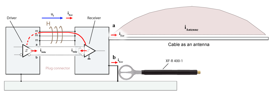
Figure 1 shows the disturbance process in a block diagram. The LVDS driver's common-mode and differential-mode currents iStör cause the emissions (Figure 1) when flowing to the receiver via the LVDS lines and pin header and return to the driver via the ground pins of the header. They generate a self-induced voltage ui in the header's ground pins. This voltage drives a disturbance current iErr across the header. This disturbance current can be driven into connected cables (Figure 1, connection a). The cables act like a transmission antenna. Connection b is used instead of connection a for the measurement. The excitation current iErr can be measured there with the XF-R 400-1 magnetic-field probe (use the current correction factor in the ChipScan-ESA software). The driver's common-mode and differential-mode currents cause this excitation current iErr and thus the emissions. They generate the excitation current iErr in the header and thereby drive the emissions.
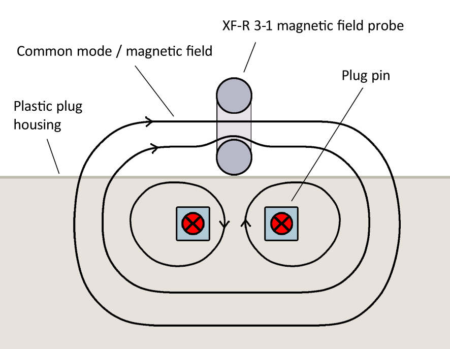
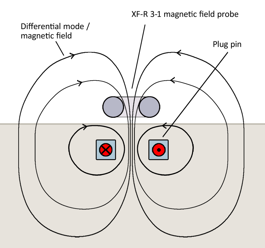
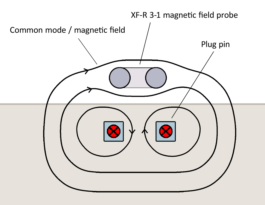
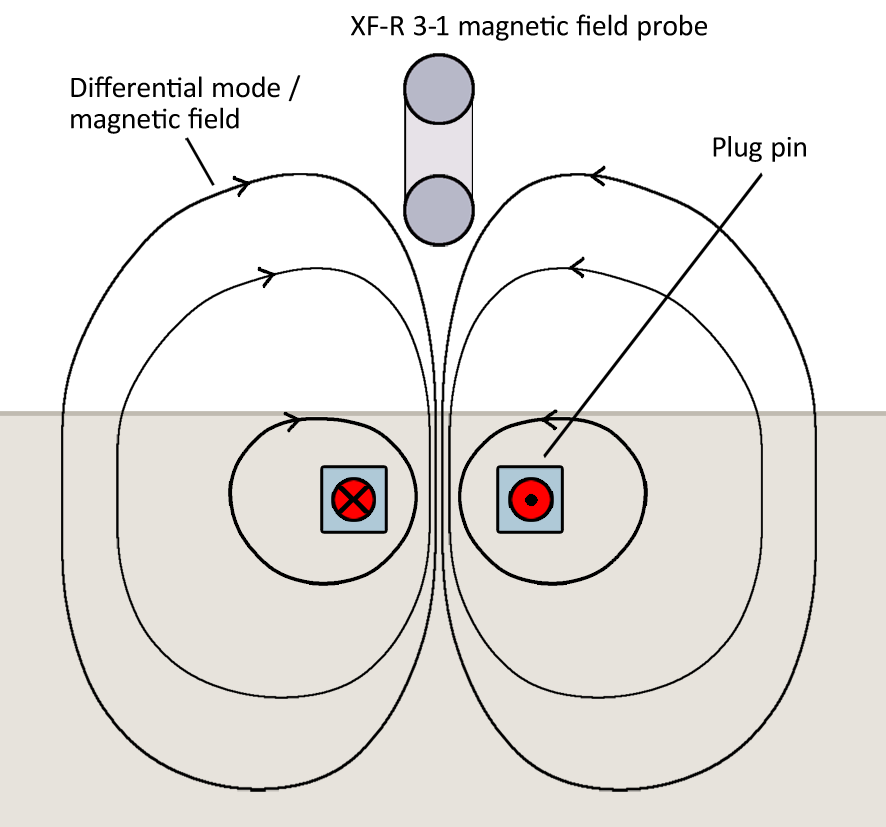
Figure 2 Measurement of common-mode and differential-mode fields on an LVDS pair with the XF-R 3-1 near-field probe
The XF-R 3-1 magnetic field probe is used to measure the common-mode and differential-mode fields on the header's LVDS lines.
Figure 2 shows the LVDS pins and how the XF-R 3-1 magnetic field probe should be arranged. Figure 2 a shows how the common-mode current is measured via the magnetic field. The near-field probe has to be held at right angles to the LVDS pair in this case. If arranged parallel to the LVDS pair, no common-mode current is measured via the magnetic field (Figure 2b).
Unlike when measuring a common-mode current, the near-field probe is held parallel to the LVDS pair to measure a differential-mode current (Figure 2c).
The figures show that common-mode and differential-mode currents can be measured selectively depending on the probe head position. Figure 3 shows the measurement results.
The differential-mode component (green) is predominant in the frequency range up to 2 GHz, whilst the common-mode component (red) is predominant in the frequency range between 2 – 4.4 GHz. The measurement results obtained with the XF-R 3-1 magnetic field probe are converted into the current iErr using the current correction factor. This conversion is carried out with the ChipScan-ESA measuring software.
 Gegentakt(gr) H-Korrektur_Chipscan-ESA_wPZ.png)
ChipScan-ESA is ideal for a comparative analysis of the measurement curves of a spectrum analyzer. The following figures only show that part of the ChipScan-ESA software user interface that is just under consideration.
Figure 4 shows the measurement set-up according to Figure 1 connection b. The header's ground pin assignment can be changed with pluggable ground pins (blue).
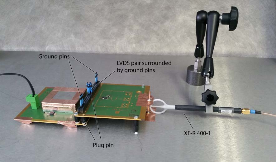
The LVDS pair is located in the middle of the header and surrounded by ground pins. The IC LVDS100 (2 Gbps) is used as an LVDS driver.
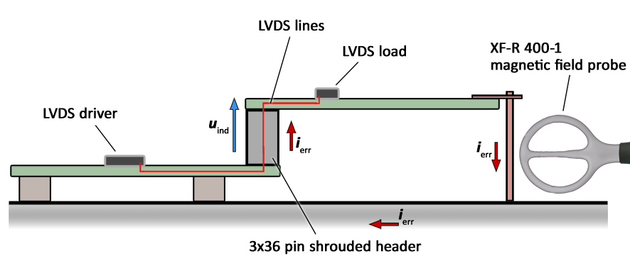
Figure 5 shows the current paths in a schematic diagram.
The following measurement steps 1 – 6 make clear how the emissions can be reduced through the header's ground pin assignment.
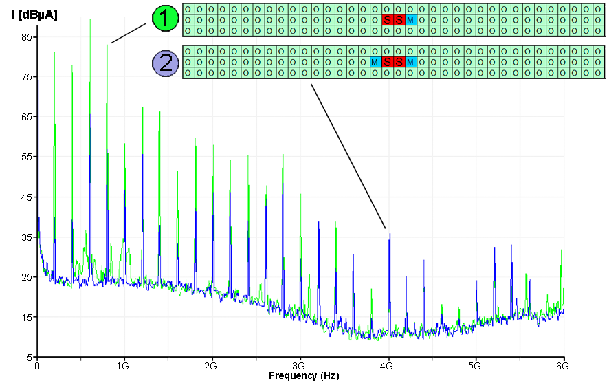
Figure 6 shows the excitation current iErr measured as a function of asymmetric (1) and symmetric (2) flanking of the LVDS pair with ground pins. The figure reveals that symmetric flanking (2) reduces the main differential-mode emission range (up to 2 GHz) (compare Figure 3). This means that a symmetric arrangement of the ground pins to flank the LVDS pair is decisive to reduce emissions. However, not only the driver currents should be kept symmetric. The example shows that the LVDS pair's environment should have a symmetric layout too.
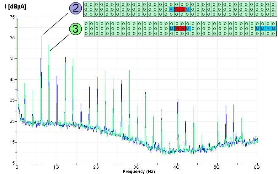
Four ground pins are used to change the symmetric ground pin assignment (2) to an asymmetric pin assignment in Figure 7 (3). Consequently, there is no clear reduction of the excitation current iErr. The emissions improve and deteriorate by a maximum value of around 10 dB with a random distribution over the entire range. Differential-mode coupling increases (deterioration) and common-mode coupling decreases (improvement) with the ground pin assignment (3). The two components' superposing effects therefore change. The components can be added to or subtracted from each other to obtain positive and negative results at the same time.
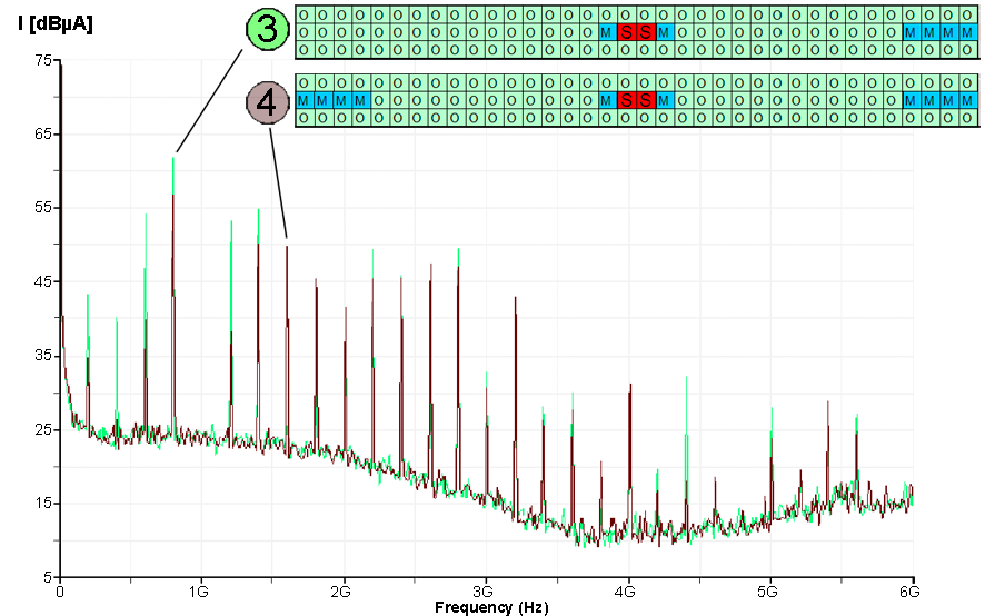
The asymmetric ground pin assignment (3) is changed to a symmetric ground pin assignment (4) in Figure 8. This results in a reduction of the differential-mode components in the frequency range up to 1.5 GHz, indicating that a symmetric ground pin assignment should also be chosen for pins that are not close to the LVDS pair.
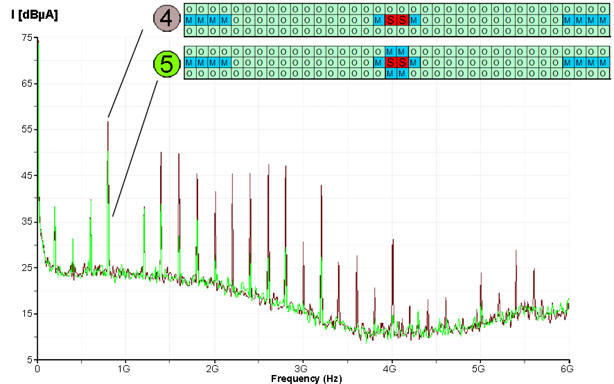
Flanking of the LVDS pair is improved with ground pins (5) in Figure 9. This results in a reduction of common-mode coupling. Since symmetry is not further improved, the ground pin assignment (5) does not influence differential-mode coupling.
Reduced common-mode coupling is particularly effective in the middle and upper frequency ranges.
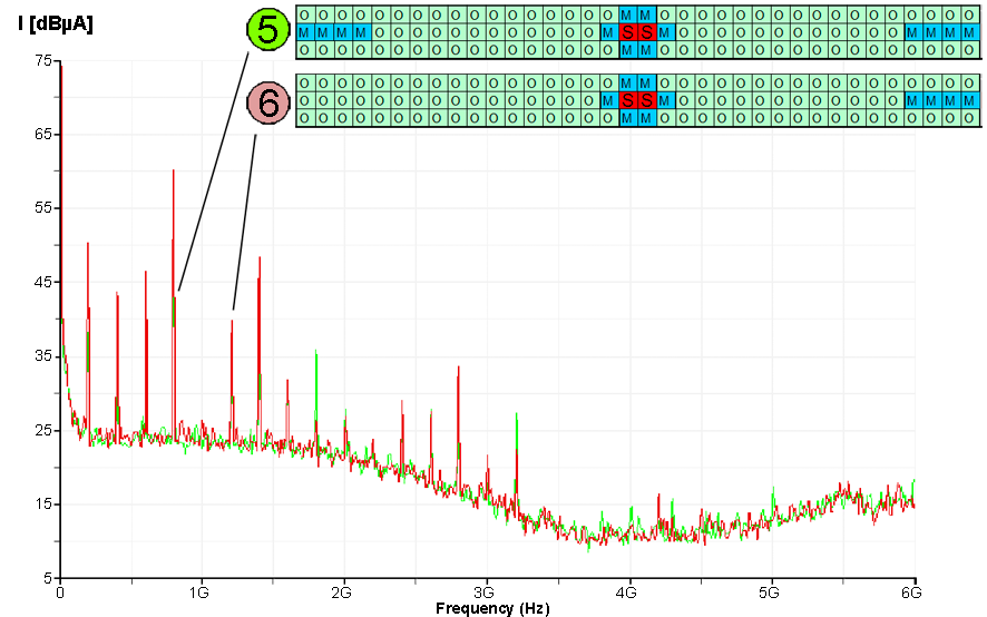
Symmetric ground pin assignment is eliminated by removing four ground pins (6) in Figure 10. This elimination of symmetry results in an increase of emissions of up to 15 dB coupled out in the range up to 1.5 GHz.
Conclusion:
Not only should the ground shielding in the LVDS pair's direct vicinity be symmetric, e.g. ground pin assignment (2), but ground pins located farther away should be symmetric too (improvement of up to 15 dB).