

Author: Stephan Pfennig
Released: 03.04.2017
Electromagnetic compatibility (EMC) is an important aspect in the development of devices and circuit boards. The essential requirements for equipment’s (devices and fixed installations) EMC are defined in the EMCD (“Electromagnetic Compatibility Directive”). In general, a distinction can be made between the interference and the immunity of an operating medium.
Part of the interference is the radiated emission. This article offers an introduction to the basic mechanics leading to the radiation-induced interference of printed circuit boards (PCBs).
Emissions and Immunity
In EMC, a simple model for describing electromagnetic interference consisting of a disturbance source, a disturbance sink, and a coupling path is typically used. The interference signal propagates from its source to its sink via the coupling path. Various coupling mechanisms can contribute to this coupling, though in principle, there is a distinction between the galvanic, capacitive, and inductive coupling as well as radiation coupling. The model distinguishes between the source interference and the immunity of the sink. Depending on the how the disturbance propagates, a further distinction is made between the line-connected- and radiated emissions and immunity, respectively. [1]
When testing electromagnetic compatibility, the device is regarded as a source of interference and an interference sink. This means that the corresponding EMC measurements are used to check whether the emissions and immunity requirements are met.
Near Field and Far Field
The measurement of the radiated interference generally takes place in the disturbance source’s far field, i.e. a certain minimum distance between the test object and the antenna is maintained during measurement. This distance is dependent on the lower limit of the frequency range. Typical measuring distances are, for example, 5 m, 10 m, and 30 m.
The fundamentals of electromagnetic radiation of antennas can be explained with the help of the electrical and magnetic elementary dipole. The so-called “2-region model”, which is based on a simplification of the equations and differentiates between the near and far field of the antenna (source), can be derived from the equations of the electric dipole (Hertzian dipole) and the magnetic dipole (Fitzgeraldian dipole). This model defines the distance r0 = λ ⁄ 2π as the boundary between the near and far field. This boundary is dependent on the wavelength λ or the frequency f. For distances r less than r0, the observed reference point lies in the source’s near field. For distances r greater than r0, it lies in the source’s far field. The distance r0 for different frequencies or wavelengths is given in Table 1. [2]
If the mentioned simplification of the equations is not used, the so-called “3-region model”, which differentiates between the near field (r < 0.6r0), the transition field, and the far field (r > 5r0), can alternatively be derived. [1,2]
| f in MHz | 30 | 48 | 100 | 300 | 1000 | 3000 |
| λ in m | 10 | 2π | 3 | 1 | 0.3 | 0.1 |
| r0 in m | 1.6 | 1.0 | 0.5 | 0.16 | 0.05 | 0.016 |
| Table 1 Near-field and far-field limits for different wavelengths and frequencies | ||||||
Furthermore, the mechanisms which lead to the radiated interference at the PCB level should be considered. The realization that the primary mechanisms (inductive and capacitive coupling) act in the near field of the printed circuit board is helpful to better understand the radiated emissions.
Mechanisms
In order to be able to minimize the radiated emissions from the PCB, it is important to understand the underlying mechanisms. The following thought-experiment is a very helpful introduction to the subject:
We assume that the size of the PCB’s dimensions is not greater than 15 cm. Furthermore, we assume that there is a broadband interference source whose amplitude spectrum has frequency components of up to about 1 GHz.
Continuous amplitude spectra with frequency components up to the gigahertz range result, for example, for non-periodic (transient) time signals with rise times in the range of a few nanoseconds. In practice, such rise times occur when switching inductances, for example.
For the second step, we assume that in the worst case, the PCB has structures that act as a λ ⁄ 2 antenna and are excited by the observed interference signal. For PCBs with dimensions d ≤ 15 cm (λ ≤ 30 cm) only frequency components f ≥ 1 GHz will be radiated directly from the PCB. This means, in the considered case there will be no radiation despite the broadband interference source. This simple example shows that interference is not typically directly radiated.
However, if there are structures in the near field of the PCB into which the electrical or magnetic near field can couple, a capacitive or inductive coupling will occur first. These structures can then act as antennas and emit the coupled interference signal. A typical example of such structures are cables connected to the PCB.
Antenna Structures
In order for the structures present in the near field to act effectively as an antenna, two conditions must be fulfilled: two elements which are not electrically small – whose dimensions are not small compared to the wavelength λ and can act together as an antenna – are required and [there must be] an interference source, which feeds the two antenna elements relative to one another. [3]
At the PCB level, various configurations which can act as a source of emission are possible. In general, two types of emission sources can be distinguished: the voltage- and current- driven interference sources. Two examples explaining these different types of interference sources are provided in the following section. [3]
Voltage Transformers and current-driven Sources of Interference
A voltage-driven interference source is present when the antenna elements necessary for the emission are fed by a disturbance voltage. The two elements could, for example, be a heat sink and a connected cable. The signal could be electrically (capacitively) coupled into heat sink by a conductor or component on the printed circuit board. If a potential difference occurs between the heat sink and the ground surface to which the cable is connected, then the interference voltage will feed these two antenna elements (heat sink and cable) and can lead to emission. [3]
An electrically long conductor train would, in principle, also be conceived as an antenna element. Typically, however, they are directly above or below a continuous ground area and thus do not effectively act as antenna elements. [3]
A current-driven source of interference is formed, for example, when conductor loops are present in the layout of the printed circuit board, the loops of which are perpendicular to the ground plane. The current flowing through a conductor loop generates a magnetic field, which also partly forms around the ground surface. This amount is dependent on the dimensions of the ground surface and causes a voltage drop between the points of the ground surface where the conductor loop is connected. If two cables which act as antenna elements are connected to the corresponding (opposite) sides of the printed circuit board, the interference voltage can lead to emission. In comparison to the useful signal, the interference voltage is typically very small, but can contribute significantly to the interference emission. [3]
Example
The operating mechanisms, which lead to radiated interference at the PBC level, are explained through many practical examples at experimental EMC seminars held by Langer EMV-Technik GmbH. The seminar uses, for example, the seminar board A62, which is equipped with a booster converter. Using the near-field probe RF-E 02, the existing electric field is measured in the frequency range from 30 MHz to 500 MHz, which can capacitively couple into other structures. The largest measured values are above the inductance of the step-up converter. The interference voltages measured at the spectrum analyzer while the near-field probe is positioned one centimeter above the inductance are shown in Figure 1. The given comparison of the measured voltage levels with the board switched on and off shows the interference potential of this voltage-driven interference source.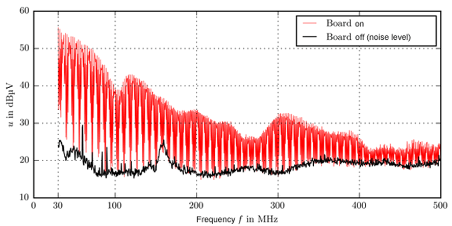
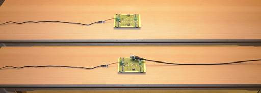
In the next step, the seminar board is placed on the table and the radiated interference in the frequency range of 30 MHz to 500 MHz is examined with a broadband EMC antenna (Bilog antenna) at a distance of 3 m. To do this, the board is placed on the center of the table with the power cable placed to the left of it. Subsequently, one end of a laboratory cable is placed at the step-up converter’s inductivity and the cable is moved to the right [of the board]. There is no electrically conductive connection between the board and the cable. The length of the table is 160 cm. The two cables hang [downward] off the end of the table.
The subsequent interference measurement (Figure 2) is displayed in two configurations – with and without the laboratory cable. Analogous to the first measurement taken with the near-field probe, the interference voltages measured at the spectrum analyser are recorded and displayed. Since a statement on the absolute field strength values was not necessary in either case, the conversion of the voltage levels is not done.
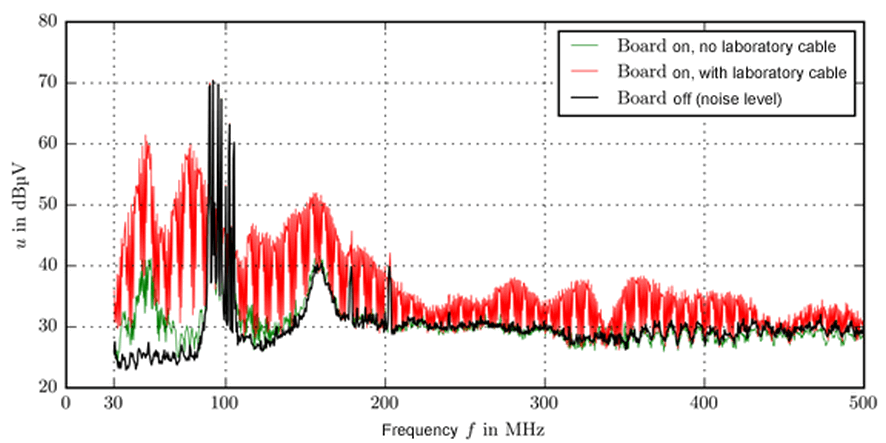
The results in Figure 3 show a significantly stronger interference when using the laboratory cable. This means the electric field measured with the near-field probe capacitively couples into the laboratory cable. Because of its length (not being electrically short), the cable acts as a second antenna element and, together with the power cable, forms an effective radiating antenna structure.
Since the interference was measured with the Bilog antenna in an unshielded space, the signals in the environment, such as FM radio signals, are included in the measurement. The corresponding frequencies, however, can be seen in the comparison between the measured noise and ambient level.
Summary
The radiated interference emitted at the PCB level are generally not emitted directly from the printed circuit board, even if corresponding sources of interference are present. Emission occurs only when the disturbance variables are coupling in to other structures which act as antennas.
In order for the structure to radiate effectively, there must be two antenna elements whose dimensions are not electrically short and are fed to one another from a disturbance source. Examples of antenna elements include: cables, heat sinks, metal rails [traces?], or other electrically conductive structures. When considering the interference source, a distinction can be made between voltage-driven and current-driven sources on interference.
In order to improve one’s understanding of interference sources, coupling mechanisms, antenna structures, and radiated-related emissions resulting therefrom, fundamental function mechanisms are explained in EMC experimental seminars offering many practical examples.
References
| [1] | A. J. Schwab und W. Kürner, Elektromagnetische Verträglichkeit, 5., aktualisierte und ergänzte Auflage, Springer-Verlag Berlin Heidelberg, 2007. |
| [2] | C. Capps, „Near field or far field?“, Delphi Automotive Systems, 16. August 2001. [Online]. Available: http://m.eet.com/media/1140931/19213-150828.pdf. [Zugriff am 20. Februar 2016]. |
| [3] | T. H. Hubing, “Printed Circuit Board EMI Source Mechanisms”, in 2003 IEEE International Symposium on Electromagnetic Compatibility, DOI: 10.1109/ISEMC.2003.1236553, 2003. |