

The EMC standard for ICs (IEC 62132) provides three typical measuring methods for such a characterisation: the DPI (Direct Power Injection) method, the TEM cell (Transverse Electromagnetic Cell) method and the use of a IC stripline.
This article examines the DPI test method in more detail. Furthermore, it explains limitations that are used as a starting point to extend this method.
The parameters obtained with the extended method describe the IC's immunity for its future practical use. The IC user can take these immunity parameters as a basis for selecting the appropriate IC for a specific electronic system and as a basis for EMC design in printed circuit board development. Furthermore, the IC manufacturer can use this information to narrow down and eliminate weak points in the chip. The article also presents a practical example: a LIN transceiver being examined using an extended DPI test method.
Further development of the DPI test method
The DPI method according to IEC 62132-4 (Figure 1) has proven successful in practice to evaluate the EMC immunity of ICs.
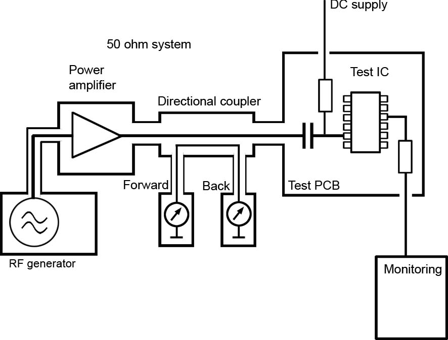
RF is injected into an individual IC pin by conductive coupling. The RF current flows from a power amplifier to the respective pin via a 50 ohm line and a coupling capacitor. The intensity of the RF disturbance is determined by the forward power that is measured with directional couplers. The power is the correct physical evaluation parameter if an RF-induced rise in temperature in the IC results in its malfunctioning.
Other RF interference events may, however, be independent of the power that is fed in. The oscillator may stop or demodulation may occur in an operation amplifier, a transistor or a diode, for example. These interference mechanisms only depend to a small degree on the power converted in the IC but they are triggered directly by basic physical parameters such as the RF current and voltage instead (example: demodulation of the RF current). The disturbance voltage or disturbance current is also the parameter responsible for driving the respective interference event in the device under test in other fields of EMC testing such as burst or ESD tests. A high current or a high voltage is not necessarily accompanied by a high power.
When testing semi-conductors, matching depends on the switching state. In addition, the switching edge has to be taken into account with its own mismatching characteristic. The averaging Pforward, Pback power measurement does not provide any system information that is relevant in terms of the u(t) and i(t) parameters. But the variation of the RF current and voltage over time is crucial for gaining new insights such as the identification of weak points in the IC and for organising counter-measures in IC design as well as in printed circuit board development.
Measuring interference with an ammeter and voltmeter
The ohmic resistance of a microcontroller power supply pin is usually small. It may be in the range between a milliohm and ohm. A capacitance of several nF may be integrated in the IC which also supplies impedances in the ohm range at 100 MHz or higher frequencies. The IC's line inductances produce similar values. Hence it follows that the IC's internal resistance is very low and may thus be considerably smaller than the 50 ohm source of the power amplifier. This means that the power amplifier operates under short-circuit conditions and then supplies its maximum current. The fed-in current interferes with the IC function but the wattmeter only shows a few milliwatt. As a consequence, the IC is evaluated as much too weak and misclassified based on the power evaluation.
The impedance of other IC pins may also be between a milliohm and kiloohm. The system approaches short-circuit conditions for IC impedances < 50 ω and open-circuit conditions for impedances > 50 ω. Immunity tests at a quasi open-circuit voltage, as are common practice in high-voltage technology, are impossible with an RF injection into an IC. The current and voltage conditions on the pin are based on the total system and must be measured directly on the pin (Figure 2).
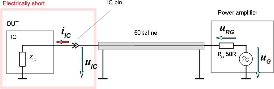
This electrically short measurement set-up avoids the metrological difficulties of standing waves that may be generated on the line to the power amplifier.
This example clearly shows RF current and RF voltage to be the decisive parameters for IC evaluation.
Figure 3 and 4 show a measurement set-up (named "P500 probe measurement system" in the following text).
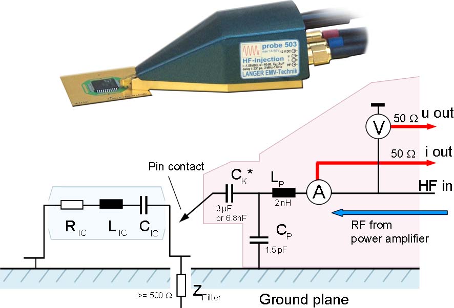
The RF disturbances flow from the power amplifier into the IC pin to be evaluated via the connected P500 probe. An ammeter and voltmeter are also integrated in this probe so that the current, voltage and phase angle can be measured with an oscilloscope. The power, impedance and other parameters of the device under test can be calculated from the measured values.
The parameters that are obtained allow engineers to draw more detailed conclusions in terms of an IC's EMC in the respective electronic system. Malfunctions that occur at high current intensities, for example, are often due to magnetic coupling while those that occur at high voltages will be due to capacitive coupling. The new measuring method allows the measurement of reactive currents that remain undetected with usual power measurement and provides detailed physical insights that were otherwise impossible. This new RF injection method with integrated current and voltage measurement is very beneficial for IC development.
Investigations on a LIN transceiver
An RF equivalent circuit can be derived for each individual IC pin from the results obtained with the P500 probe measurement system. The impedance of the pin, however, depends not only on the switching state of the signal but also on the RF generator voltage. The P500 probe is used to inject a small RF level into the pin. These disturbances must be low enough to prevent protection diodes from opening and additional current paths and elements from becoming effective, for example. On the basis of the U, I and φ values measured with the oscilloscope, the IC's resistance and reactance can be determined as a function of frequency. If there is no dominant capacitive or inductive share, the reactance can be split in XC und XL by calculation. This requires measurements at different frequencies.
Weak points can be found in the IC through a high-frequency / low-frequency current and voltage analysis on the IC pin. The high-frequency voltage may cause diode paths, for example, to open, resulting in a change in impedance.
The measurement system can be used for a variety of practical analyses. For example, it allows the visualisation of time-varying non-sinusoidal high-frequency current and voltage waveforms(Figure 5).
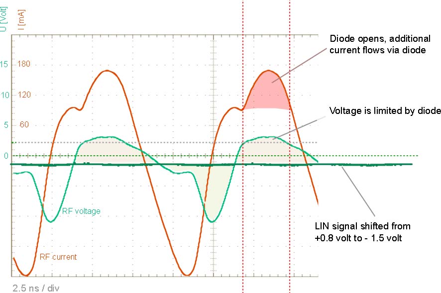
Additional current paths will open as soon as the forward voltage of internal diodes is reached. The impedance of the IC drops, the current increases and the voltage can be limited (feedback to supply network). When a diode opens, new coupling paths can become effective. The current that flows through the diode enters other network sections and takes effect there as a rectified current. These currents or voltages superimpose useful signal such as trigger or control signals of the LIN driver and cause the FET to go into a blocked, an open or undefined state. Further IC-internal mechanisms of actions can be clarified by analysing current and voltage as a function of time. Manufacturers can launch a targeted IC improvement and users can derive EMC counter-measures for the IC's practical use.
Conclusions for module development
A sensitive IC can become a victim of interference if an RF current couples to susceptible pins via internal coupling paths in the layout, for example. The RF current may flow from a vehicle board network plug to the Vbat pin of the LIN transceiver via corresponding line connections. The RF current may also reach the GND pin via the GND system, particularly in the segmented GND of two-layer printed circuit boards. This coupling path can be blocked by an all-over contact GND system. In addition, the blocking capacitors have to be adequately dimensioned on Vbat. A filter structure that comprises an inductor and two filter capacitors (PI filter) is a recommended option. The filter prevents the RF current from reaching the sensitive pin. Such a measure can be taken with due care right at the beginning of development if the Vbat pin is known to be very sensitive.
Interference suppression on a module that comprises LIN transceivers is difficult in practice as the respective pins which are finally responsible for IC interference have to be identified. The situation becomes unclear if the IC has several sensitive pins that all contribute to its malfunction. The effectiveness of individual measures is concealed due to coupling to other pins. If the IC's sensitive pins are known, reliable counter-measures can be taken in the right place even before beginning the actual EMC work. EMC problems of ICs can thus be controlled more quickly and easily.