


User manual
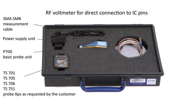
P700 probe set
RF voltmeter for direct connection to IC pins
Inhalt
1 P700 probe
This probe is an RF voltmeter and is used to measure RF voltages on IC pins It is ideal for measurements in unmatched systems (with source impedances unequal to 50 Ohm such as IC pins).
The voltmeter comprises the P700 basic unit and exchangeable TS probe tips.
The probes' internal resistance is their distinguishing feature. The TS 701 probe tip has the highest internal resistance of 1.5 kOhm. The TS 705 probe tip has the lowest internal resistance of 50 kOhm.
The voltmeter is used to measure the conducted electromagnetic emissions of integrated circuits in accordance with IEC 61967. The RF voltage is measured directly on the IC pin with a 150 Ω coupling network. The coupling network is integrated in the TS 751 probe tip.
The TS 701 probe tip with an internal resistance of 1.5 kOhm is available for measurement tasks requiring a high-resistance voltmeter. The TS 705 (50 Ohm) and 706 (100 Ohm) probe tips can be used for measurement tasks with a low-resistance voltmeter or for matched measurements. The TS 705 can be used to measure systems that are matched to 50 Ohm.
Electromagnetic emission measurements that are carried out with the P700 probe and the corresponding probe tip ensure a very precise repeatability and comparability.
The IC pins to be measured are defined in the layout of the test board for measurement set-ups in accordance with IEC 61967. This means that the measurement set-up is determined for and restricted to a few pins.
The P700 probe tip is used to contact the IC pin directly during the measurement. The probe is easy to handle and allows the user to contact any pin quickly and precisely.
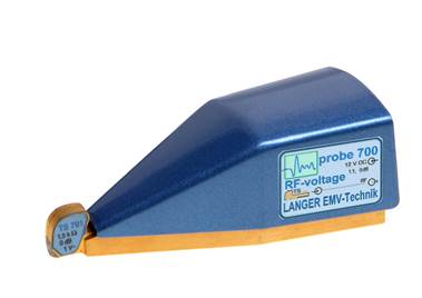
1.1 Design and function of the P700 probe
1.1.1 P700 basic unit
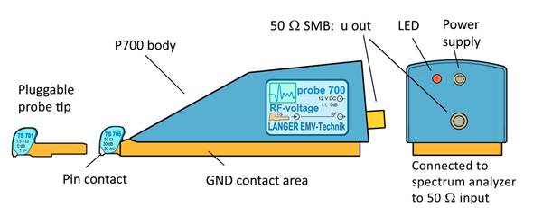
The P700 is a basic probe unit (Figure 3 Internal design of the P700 probe) which is only operational after fitting one of the probe tips. The probe's GND contact surface ensures low-impedance, all-over contact with the GND 25 ground plane (TS 1002 test bed). Magnets that are integrated in the probe hold it on the ground plane. The user can thus contact the selected IC pin easily and precisely.
The P700 probe has a 50 Ohm SMB socket (50 Ohm SMB: u out, Figure 2) at its rear end to connect a measuring instrument such as a spectrum analyzer. The measurement signal is coupled out of the probe via the SMB socket.
Weiterhin besitzt die Probe P700 hinten einen 3,4 mm Stromversorgungsanschluss für ein 12 V Steckernetzteil. Die LED signalisiert die Stromversorgung der P700. Die Stromversorgung dient der Speisung der Tastspitze.
Furthermore, the P700 probe has a 3.4 mm power supply connection at its rear end to connect a 12 V power supply unit. The LED signals the P700's power supply. The power unit supplies the probe tip.
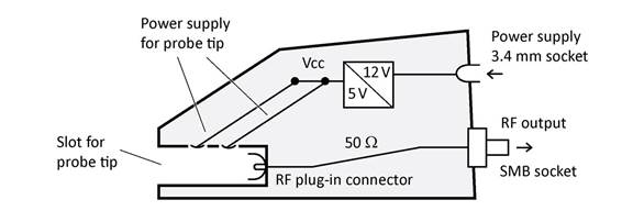
A slot to hold one of the four probe tips (TS 701, TS 705, TS 706, TS 751) is located at the front end of the P700 probe. There are two contacts in the upper part of the slot via which the probe tip is supplied with power. The amplifier that is integrated in the probe tips is supplied with a controlled voltage of 5 V.
An RF plug-in connector is located at the rear of the slot. A 50 Ohm matched line transmits the measurement signal from there to the SMB output (Figure 2).
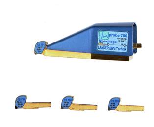
1.1.2 Probe tips
The probe tip is plugged into the probe unit from the front. The probe is now operational.
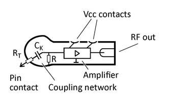
The pin contact that is used to contact the IC pin for the RF voltage measurement is located at the probe tip.
The probe tip includes a coupling network. This coupling network picks up the RF voltage from the IC pin via the pin contact. It also includes a divider with a coupling capacitor. The divider's dimensional design determines the input resistances and divider factors of the different probe tips.
The divider's output is connected to an amplifier. The amplifier boosts the measurement signal and is supplied with power via the P700 basic unit and the two aforementioned contacts. The amplifier output is connected to an RF socket which makes contact with the P700 probe when the probe is plugged in.
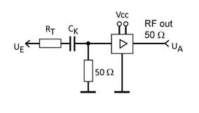
Figure 5 shows the probe tip's internal circuit.
The capacitor Ck is used as a DC disconnector between the test IC and the probe.
1.2 Characteristics of the P700 and probe tips
1.2.1 P700 basic unit
| P700 | P700 basic unit |
|---|---|
| RF input | Special plug-in contact to the TS probe tips |
| RF measurement output | SMB, 50 |
| Auxiliary energy | 12 V |
1.2.2 Probe tips
The measurement output of the probe tips is isolated from the measurement divider by a 30 dB pre-amplifier.
The probe tip's low capacitance (TS 701's cross-over coupling capacitance: 0.3 pF) reduces transient phenomena at low-impedance sources. The probe tip's measuring contact is connected to its internal resistor at low inductance (L « 1 nH).
A special characteristic of the TS 705 probe tip: the input resistance is 50 ω. The connection to the probe tip's internal resistor is approx. 4 mm long. The measuring cable is isolated from the pin contact by a pre-amplifier. No reflexion processes occur in the measuring cable with a mismatched device under test.
1.3 The P700 in the test bed
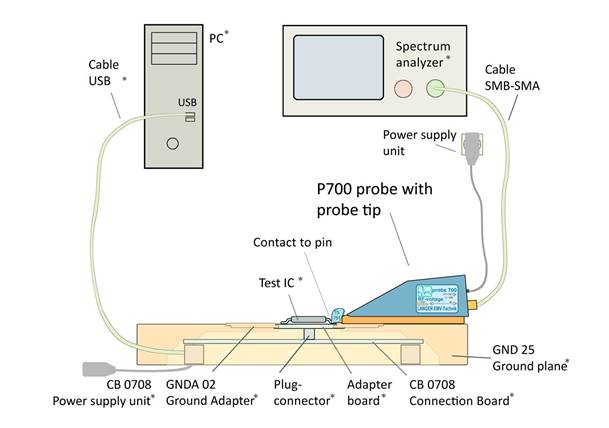
The components marked * are not included in the scope of delivery.
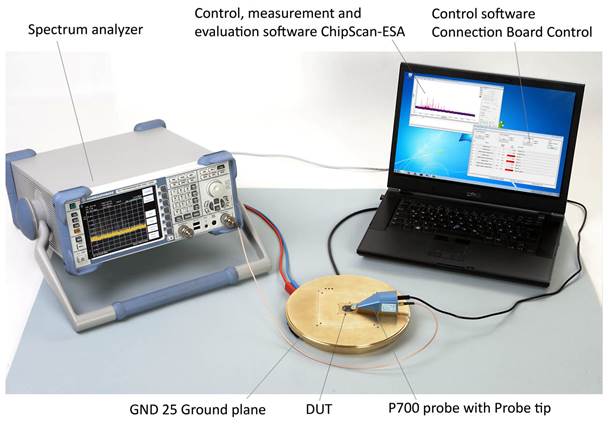
Figure 6 shows the set-up of the IC test system with the ICE1 test bed and the P700 probe set. The test IC is mounted on an adapter board. The adapter board is inserted into the ground plane and connected to the connection board via a plug connector. The ground plane and the connection board are integral parts of the ICE1 IC test bed. The evaluation of signals from the test IC may require external devices such as a spectrum analyser or special test hardware (Figure 6).
The test IC can be operated on the adapter board autonomously or controlled via the connection board. The software connection board control that is used to control the test IC is installed on the PC.
The probe tip of the P700 probe is brought into contact with a pin of the test IC through its pin contact. The measurement signal is transmitted to a spectrum analyzer via the SMB-SMA cable.
The values that are picked up and measured can be transmitted from the spectrum analyzer to a PC connected to the test set-up. The ChipScan-ESA software from Langer EMV-Technik GmbH allows the operator to record, colour, annotate, calculate or individually visualise any number of measurement curves of a spectrum analyser and thus compare them quickly and easily. To receive the ChipScan-ESA viewer free of charge, please contact us at:mail@langer-emv.de
The devices listed in the table are described in their respective operating instructions:
| Task | Operating instructions | |
|---|---|---|
| IC-EMV Anleitung (Langer EMV-Technik GmbH) | |
| ICE1 user manual | |
2 Safety instructions
When using a product from LANGER EMV Technik GmbH, please observe the following safety instructions to protect yourself from electric shocks or the risk of injuries.
The device may only be used by personnel who are qualified in the field of EMC and who are fit to work under the influence of disturbance voltages and (electric and magnetic) burst fields.
Read and follow the user manual and keep them in a safe place for later consultation.
- Never use any damaged or defective devices.
- Carry out a visual check before using a measurement set-up with a Langer EMV-Technik GmbH product. Replace any damaged connecting cables before starting the product.
- Never leave a Langer EMV-Technik GmbH product unattended whilst this is in operation.
- The Langer EMV-Technik GmbH product may only be used for its intended purpose. Any other use is prohibited.
- Observe the operating and safety instructions for all devices used in the set-up.
- People with a pace-maker are not permitted to work with this device.
- The test set-up should always be operated via a filtered power supply.
- Attention! Functional near fields and interference emissions may occur when operating EMC test set-ups. The user is responsible for taking measures to prevent any interference to the correct function of products outside the EMC environment of the test set-up (in particular through radiated interference).
- This can be achieved by:
- observing an appropriate safety distance,
- use of shielded or shielding rooms.
- The disturbances that are injected into the ICs can destroy (latch-up) the device under test if their intensity is too high. Protect the device under test by:
- increasing the disturbance gradually and stopping when a functional fault occurs,
- interrupting the power supply to the device under test in the event of a latch-up.
Attention! Make sure that internal functional faults are visible from outside. The device under test may be destroyed due to an increase in the injection intensity if the faults are not visible outside. Take the following measures as necessary :
- monitoring of representative signals in the device under test,
- special test software,
- visible reaction of the device under test to inputs (reaction test of the device under test).
We cannot assume any liability for the destruction of devices under test!
3 Warranty
Langer EMV-Technik GmbH will remedy any fault due to defective material or defective manufacture, either by repair or by delivery of replacement, during the statutory warranty period.
This warranty is only granted on condition that:
- the information and instructions in the user manual have been observed.
The warranty will be forfeited if:
- an unauthorized repair is performed on the product,
- the product is modified,
- the product is not used according to its intended purpose.