

Manual
MP CI
Coupling inductance measurement set
1 Introduction
The MP CI coupling inductance measurement set is used to measure the EMC characteristics of connectors and cables. It helps to determine the coupling inductance of connectors and thus speeds up their development in terms of EMC.
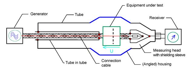
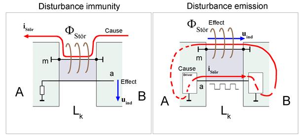
These measurements are carried out against the practical background that high-frequency signals escape from the connector and may cause disturbances (Figure 1). Disturbances may also enter the connector from the outside and interfere with the device.
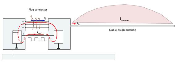
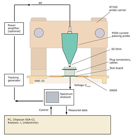
The coupling process can be technically described with the coupling impedance R or the shield attenuation a (Figure 2). The coupling impedance can be measured with the tube-in-tube method (Figure 3). A high-frequency current is coupled into a signal pin of the connector with an RF generator. A voltage U is transferred to the connector's shielding housing via the coupling impedance (frequency response Figure 2). The voltage U that is present on the outside of the connector is measured with the measuring head and receiver. The ratio of the voltage measured and the generator current is the frequency-dependent coupling impedance (Figure 2).
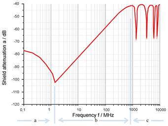
The coupling impedance ( Figure 2 ) can be divided into three frequency sections. Section A includes the ohmic voltage drop across the shielding system of the connector in the lower frequency range. Section B describes the voltage drop on the coupling inductance of the connector in the medium frequency range.
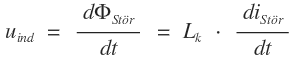
The voltage drop on the coupling inductance is described with (Eqn 1).
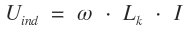 | Eqn 1 |
The connector (or cable, respectively) changes from an electrically short to an electrically long condition in section C.
Being a function of ω the voltage rises by 20 dB per decade in section B (Eqn 1). The coupling inductance Lk is a frequency-independent constant. A frequency-independent constant (Lk) is an EMC parameter that is much easier to handle than a frequency-dependent quantity (Figure 2). The development process thus becomes much more expedient.
Section B ( Figure 2 ) is relevant for emissions from the connector and its immunity. Determining the coupling inductance Lk is usually sufficient. The measurement set-up ( Figure 3 ) can be simplified due to the correlation (Eqn 1), but only to the extent that the connector remains easily accessible. This allows quick and flexible measurements in the development process and means that the connector can even be modified quickly during the tests.
2 Design and function
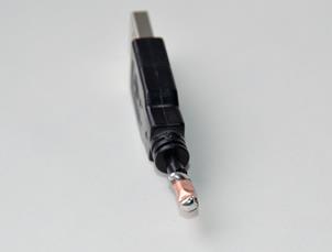
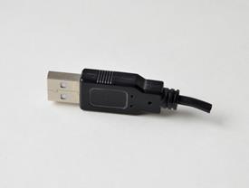
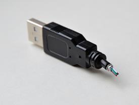
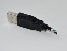
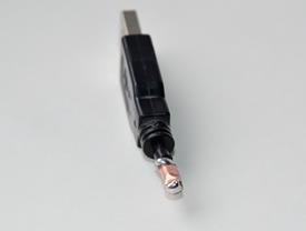
P550 transfer probe:
| Connection | Type of connection |
|---|---|
| Input of the RF signal | SMA |
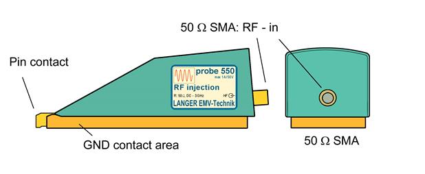
The P550 probe contains an RF-compliant, longitudinal 50 Ohm resistor for the frequency range between 0 and 3 GHz
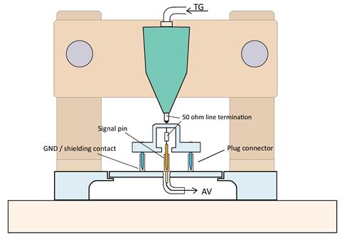
Figure 5 shows the simplified measurement set-up that is used to measure the coupling inductance Lk. The measurement current is supplied by the tracking generator (TG) of a spectrum analyzer and fed into the housing (ground reference) of the connector via the P550 transfer probe with a 50 Ohm line termination. The measurement current that is fed in induces the voltage uind across the coupling inductance Lk of the ground and shielding contacts.
The voltage uind is picked off via a 50 Ohm line termination and forwarded to the input of the spectrum analyzer (AV). The induced voltage uind depends on the geometrical structure of the ground / shielding contacts and the position of the signal pin in the connector. The inductive linkage ( Figure 6) Lk is the ratio between the current that flows via the ground / shielding contacts and the voltage induced on the signal pins.
The degree of interlinkage is described by the value of Lk.
The coupling inductance Lk (Eqn 1) is calculated in the ChipScan-CI software with the 'coupling inductance' tool on the basis of the measured curve.
3 Measuring the coupling inductance
3.1 Equivalent circuit diagrams
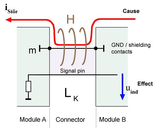
The coupling inductance describes how disturbance currents that are carried by the cable and/or connector shields are coupled inductively with the signal lines inside the cable or connector. This coupling takes place via a magnetic field. The coupling inductance Lk is identical for emissions and immunity.
Flux linkage istör relative to uind
 | Eqn 2 |
 | Eqn 3 |
Coupling inductance in differential systems
A distinction is made between the two coupling modes in differential systems.
- Common mode: describes how pairs of lines are subjected to currents that flow in the same direction with the same absolute value.
- Differential mode: describes how pairs of lines are subjected to oppositely directed (differential) currents. Thus, the disturbance voltage that is induced affects the differential data signal directly.
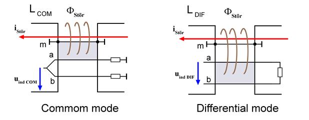
Both common mode and differential mode interference are characterised by their own respective flux linkage (Figure 8). The disturbance current iStör is coupled to the induced common-mode voltage Uind COM via the common-mode inductance LCOM and also to the induced differential-mode voltage Uind DIF via the differential mode inductance LDIF. Thus, there are two parameters (LCOM , LDIF) to describe the EMC characteristics of a connector that carries differential signals.
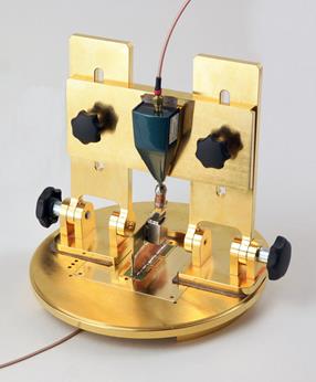
3.2 Measurement set-up
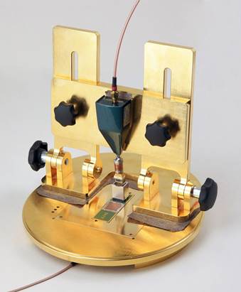
Figure 9 shows a photo and Figure 10 a schematic diagram of the measurement set-up.
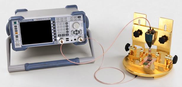
The measurement set-up comprises:
- GND25 ground plane
- KT102 probe carrier
- GNDA ground adapter (the size depends on the size of the object to be measured)
- P550 50 Ohm wheeling probe
- SMA-SMA 1 m measuring cable
- SMA-SMB 1 m measuring cable
- Test board
- Spectrum analyzer (with tracking generator)
- Power amplifier (optional)
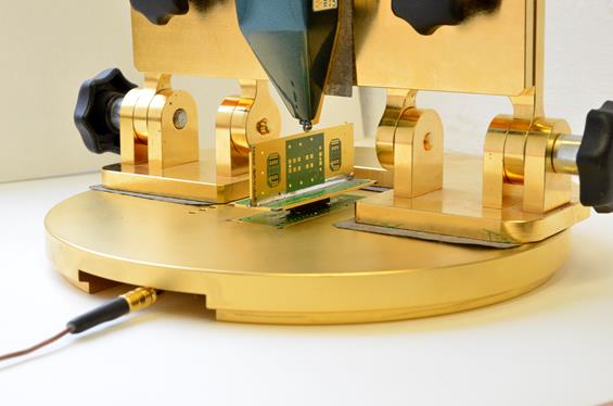
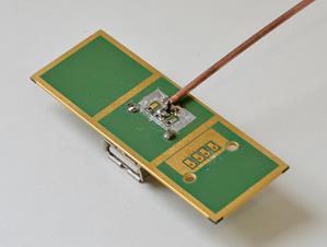
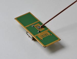
3.2.1 Test board
The test board is used as a carrier for the connector (equipment under test). Selected signal pins and ground / shielding pins are contacted on the test board via soldered connections.
Both parts of the connector have to be connected to a separate test board (Figure 13) if a board-to-board connector is measured. The board's soldered connection has to be linked to the test board if a board-to-cable connector is used (Figure 12).

3.2.1.1 Design of the test board
Four ground adapters with different sized openings are available to secure the test board. Test board size selection depends on the size and number of pins of the connector under test.
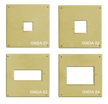
| Variant | Width / mm | Length / mm | Thickness of the test board without solder resist / mm | Tolerance |
|---|---|---|---|---|
| 1 | 22.7 | 22.7 | 1.0 | ± 0.1 mm |
| 2 | 32.7 | 32.7 | 1.0 | ± 0.1 mm |
| 3 | 22.7 | 68.1 | 1.0 | ± 0.1 mm |
| 4 | 100.0 | 100.0 | 1.7 | ± 0.2 mm |
| Table 1 Test board dimensions | ||||
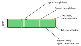
Surface:
- Project all of the connector pins from the top to the bottom layer via plated through-holes. Test signals can thereby be assigned at random if corresponding load resistors / terminating resistors are fitted.
- Use the footprint of the connector.
- Fill up the top and bottom layer with consistent ground areas ( Figure 16).
- Connect the top and bottom layer of the circuit board to each other via a close mesh of ground through-holes.
- Metallise the edges of the circuit boards.
- Enclose the pads with ground as much as is technically feasible.
- Design the adjustment bores as through-holes.
- Provide contact surfaces for the shields of the pads, load resistors and terminating resistors.
- Keep the contact surfaces for the GND adapter free of solder-resist.
3.2.2 Connection of the test board
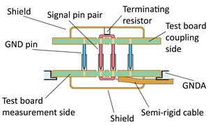
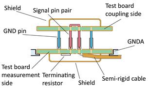
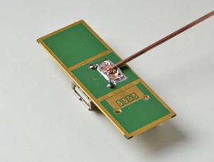
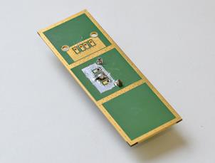
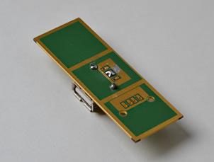
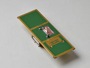
The completely assembled connector has two connection sides. The P550 is used to couple into the upper side that is shown in Figure 17 to Figure 19. The upper side will be called the coupling side in the following.
The side that is inserted into the GNDA is called the measurement side.
3.2.2.1 Connector for TTL signal
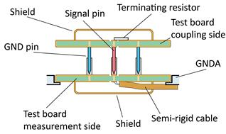
The two parts of the connector have to be connected differently to measure the coupling inductance ( Figure 17). The TTL signals to be measured are terminated with a 50 Ohm resistor on the connector's coupling side. The signals to be measured are picked off via an RF line (semi-rigid coaxial cable; SG SMB 10 cm) on the connector's measurement side. The TTL signal circuit is protected against disturbances by a closed shield. This shield is fitted on both the coupling side and the measurement side of the test board. The shield must be metal and completely closed. This can be implemented through a circumferential soldered connection.
A heavily shielded cable has to be used to lead the measurement signal out of the shielding to ensure an interference-free transmission of the TTL measurement signal. Figure 20 shows how semi-rigid lines are used to ensure proper shielding. The ground or shielding contacts of the connector are connected to ground on both the coupling side and the measurement side.
3.2.2.2 Connector for symmetric signals
Connectors for symmetric signals have the coupling inductances LCOM and LDIF (Figure 8). Two different circuits (Figure 8) are required to determine the coupling inductances. Consequently, two sets of test boards are required. One set of test boards is needed to determine LCOM and another set of test boards is needed to determine the coupling inductance LDIF.
3.2.2.3 Common-mode configuration for symmetric signals
The two parts of the connector have to be connected differently to measure the coupling inductance LCOM (Figure 19). The two lines that carry the symmectric signal are connected and terminated with a 50 Ohm resistor on the coupling-side connector part. The two lines that carry the symmectric signal are also connected on the measurement-side connector part and the signals are picked off via a (semi-rigid) RF line. The circuit is protected from disturbances by a closed shield. This shield is fitted on both the coupling side and the measurement side of the test board. The shield must be metal and completely closed.
This can be implemented through a circumferential soldered connection.
A heavily shielded cable has to be used to lead the measurement signal out of the shielding to ensure an interference-free transmission of the measurement signals. Figure 20 shows how semi-rigid lines are used to ensure proper shielding. The ground or shielding contacts of the connector are connected to ground on both the coupling side and the measurement side.
3.2.2.4 Differential-mode configuration for symmetric signals
The two parts of the connector have to be connected differently to measure the coupling inductance LDIF (Figure 19). The two lines that carry the symmetric signal are bridged on the coupling-side connector part. One of the two lines that carry the symmetric signal is terminated with a 50 Ohm resistor on the measurement-side connector part. The other line is connected to the semi-rigid cable (Figure 19). The circuit is protected from disturbances by a closed shield. This shield is fitted on both the coupling side and the measurement side of the test board. The shield must be metal and completely closed. This can be implemented through a circumferential soldered connection.
A heavily shielded cable has to be used to lead the measurement signal out of the shielding to ensure an interference-free transmission of the measurement signals. Figure 20 shows how semi-rigid lines are used to ensure proper shielding. The ground or shielding contacts of the connector are connected to ground on both the coupling side and the measurement side.
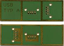
3.2.2.5 Design of the measurement-side test board taking a USB connector as an example
The USB connector has pin pairs for symmetric signals. Two sets of test boards are designed according to Figure 7 and according to Figure 18 and Figure 19.
| Common Mode | Differential Mode |
|---|---|
| 1. The connector is fitted on the measurement-side test board, top layer. | 1. The connector is fitted on the measurement-side test board, top layer. |
| 2. All ground and shield contacts of the connector are connected to the test board ground. | 2. All ground and shield contacts of the connector are connected to the test board ground. |
| 3. The connections of the signal pair are joined and then connected to the signal line of the semi-rigid cable. | 3. One signal connection of the signal pair is terminated with a 50 Ohm resistor and the other one is connected to a semi-rigid cable on the bottom layer. |
 |  |
| 4. Further signal pairs can be treated in the same way. | 4. Further signal pairs can be treated in the same way. |
| 5. The whole circuit area is shielded with Cu foil. The Cu foil is soldered to a soldering area that has been prepared on the test board. The sheath of the semi-rigid cable is soldered to the Cu foil along its circumference. | 5. The whole circuit area is shielded with Cu foil. The Cu foil is soldered to a soldering area that has been prepared on the test board. The sheath of the semi-rigid cable is soldered to the Cu foil along its circumference. |
 |  |
3.2.2.6 Design of the coupling-side test board
| Common Mode | Differential Mode |
|---|---|
| 1. The connector is fitted on the coupling-side test board’s top layer. | 1. The connector is fitted on the coupling-side test board’s top layer. |
| 2. The connections of the signal pair are joined and terminated with a 50 Ohm resistor on the bottom layer. | 2. The signal connections of the signal pair are bridged on the bottom layer. |
 |  |
| 3. Further signal pairs can be treated in the same way. | 3. Further signal pairs can be treated in the same way. |
| 4. The whole circuit area is shielded with Cu foil. The Cu foil is soldered to a soldering area that has been prepared on the test board. | 4. The whole circuit area is shielded with Cu foil. The Cu foil is soldered to a soldering area that has been prepared on the test board. |
 |  |
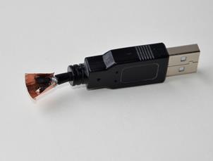
3.2.2.7 Preparation of the coupling-side cable connectors taking a USB connector as an example
Table 2: Cable connector, common-mode
| Common Mode | Description |
|---|---|
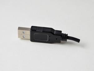 | Figure 28 Cut the cable so that a piece approximately 1 to 2 cm remains. |
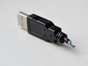 | Figure 29 Remove the cable sheath. |
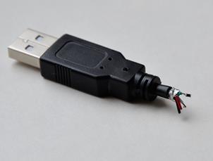 | Figure 30 Fold the shielding outwards. |
 | Figure 31 Bridge the wire pair to be measured and terminate with a 50 Ohm resistor (the cable shield is the reference contact). |
 | Figure 32 Shield the entire cable end with Cu foil (solder the terminating resistor to the Cu foil and insulate the signal cores) |
Table 3: Cable connector, differential mode
| Differential Mode | Description |
|---|---|
 | Figure 33 Cut the cable so that a piece of approximately 1 to 2 cm remains |
 | Figure 34 Remove the cable sheath |
 | Figure 35 Fold the shielding outwards The core pair to be measured is bridged. |
 | Figure 36 Shield the entire cable end with Cu foil (insulate the bridged signal cores against ground) |
3.3 Performing the measurement
Since the coupling inductance is determined by the magnetic field distribution in the connector under test, many factors that may affect the measurement have to be taken into account. The coupling inductances of a connector's signal pins will be different. Metal parts that are fitted next to the connector may also alter the coupling inductance in special cases. The potential influence of adjoining metal parts on the coupling inductance has to be checked when assessing the practical use of connectors.
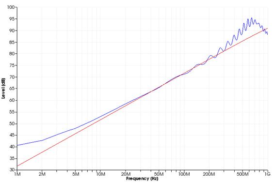
The coupling inductance is a frequency-independent constant. It is, therefore, sufficient to analyze one measuring point. The measuring point may be located in a wide frequency range. The frequency response has to be checked to locate the linear range that could be used for a measuring point. In practice, a straight line is placed in the frequency response characteristic so that it coincides with the linear section.
Due to the limited sensitivity of the measurement device (spectrum analyzer), there is a deviation from the linear curve in the lower frequency range.
Transients will occur in the upper frequency range due to the open measurement set-up and the parasitic elements that become thereby effective. These effects determine the upper measurement limit. The useful frequency range is between around 1 MHz – 500 MHz. The coupling inductance is a constant in this range. The frequency response of the measurement signal is, thus a linear function if a double logarithmic scale is used.
We suggest the following measurement process:
- Set up the measurement equipment as shown in Figure 10
- Insert the measurement side of the fitted test board into the ground adapter (GNDA 01-04) and fix with adhesive copper (Cu) tape.
- Plug in the coupling side test board or the cable connector
- Switch on the measurement device and the PC.
- Connect the measurement device to the PC
- Start the ChipScan-CI.
- Adjust the ChipScan-CI and the measurement device → 3
- Normalise the measurement device to the measurement set-up
- Connect the ends of the cables to the interfaces of the measurement set-up (P550 and test board coupling side)(see Figure 10)
- Establish the contact between the P550 probe and the coupling-side test board or cable plug.
- Record the measurement curve.
- Analyse the measurement curve with the ChipScan-CI 'coupling inductance' tool
The measurement value has to be recorded sequentially if there are several signals per connector. The cable has only to be connected to another measurement device entry for this purpose.
4 Operating the ChipScan-CI
4.1 Basic ChipScan-CI operation
The basic operation / installation of ChipScan-CI is described in the respective software manual.
Start ChipScan-CI
Search and integrate the measurement device
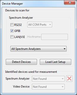
- Menu → Devices → Device Manager
- Adjust the interface (RS232, GPIB, LAN). Click 'Detect Devices'
- Adjust the spectrum analyzer via the 'Spectrum Analyzer Manager' console and directly on the spectrum analyzer.
- Normalise the spectrum analyzer
- Connect the free end of the cables that are connected to the measurement device
- Click on the 'Normalise' button in the 'Spectrum Analyzer Manager'
- Split the connection 5
- Record the measurement value
- Connect the free end of the generator cable to the P550 input
- Bring the P550 into contact with the coupling point (shield) of the coupling-side test board
- Connect the measurement output of the measurement-side test board to the measurement input of the spectrum analyzer
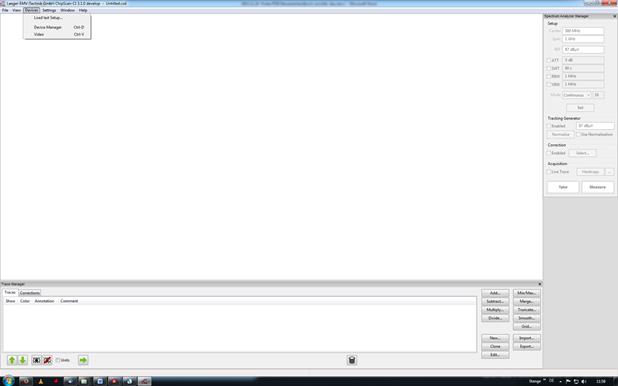
Your measurement device appears in the list: 'Identified devices used for measurement' Close the 'Device Manager'
Basic settings for the measurement:
Table 4: Basic settings of the spectrum analyzer to measure the coupling inductance
| Parameter | Value | Where this is set |
|---|---|---|
| Span | 1 GHz | Spectrum Analyzer Manager |
| Center Frequenz | 500 MHz | Spectrum Analyzer Manager |
| Tracking Generator Level | 100 dBµV | Spectrum Analyzer Manager |
| RBW / VBW | 100 kHz / 300 kHz | Spectrum Analyzer Manager |
| Reference Level | 100 dBµV | Spectrum Analyzer Manager |
| Mode | Continuous oder Average | Spectrum Analyzer Manager |
| Internal Preamplifier | ON | Directly at the spectrum analyzer |
| Input Impedance | 50 Ohm | Directly at the spectrum analyzer |
NOTE: The required settings depend on the used spectrum analyzer and the quality of the device under test
→ The entries in the 'Spectrum Analyzer Manager' only become effective by clicking the 'Set' button.
Click the 'Measure' button in the 'Spectrum Analyzer Manager' to transfer the measured values to the PC
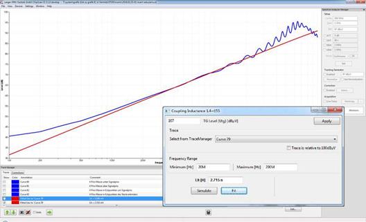
4.2 Using the Coupling Inductance ChipScan-CI tool
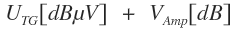
The following sequence describes how the coupling inductance Lk EMC-parameter is created from the measured data by the 'Coupling Inductance' tool that is integrated into Chipscan-CI.
- Start the ChipScan-CI software and load the measured data (.csd)
- Start the tool: 'Coupling Inductance' in the title menu → Window/'Coupling Inductance'
- Only enter the tracking generator voltage UTG [dBµV] in the 'TG Level' field (for a measurement set-up without power amplifier)
- If a power amplifier is used, enter the sum of the tracking generator voltage and gain of the power amplifier in the 'TG Level' field.
- Apply and confirm the entry and confirm by clicking 'Apply'.
- Select the measurement curve to be fitted
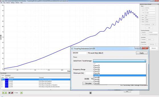
- Enter the window limits for automatic fitting 'Frequency Range' Figure 42 by entering the minimum and maximum frequency
- Start the calculation via 'Simulate' and 'Fit'
- The fitted curves are stored in the 'TraceManager' and the coupling inductance is stored in the curve's comment box.
 | Eqn 4 |
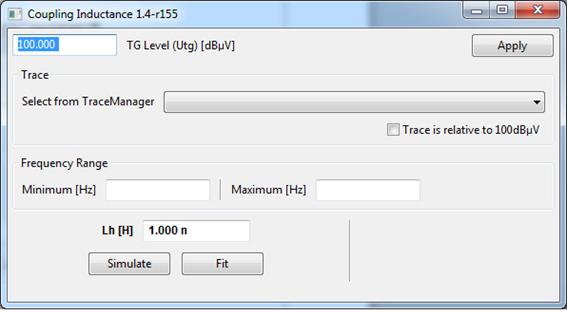
- The 'Select from TraceManager' dropdown box contains all curves that are also contained in the 'TraceManager' (Figure 40)
Symbols:
| k | 103 |
| M | 106 |
| G | 109 |
'Simulate': simulates the straight inductance line with the value entered in Lh [H].
→ This allows you to approach the curve manually.
'Fit': starts the recursive nestling of the straight inductance line to the measurement curve
→ Extraction of the coupling inductance and display in in Lh [H]
| p | 10-12 |
| n | 10-9 |
Note:
This measurement example clearly shows how the curve deviates from the linear curve in the frequency range 0 – 20 MHz and how the measurement curve is distorted in the frequency range 400 – 1000 MHz on account of the connector's shielding resistance.
Thus, special attention has to be paid to the curve of the straight inductance line during analysis. A family of curves can be generated quickly by matching the evaluation frequency range.
5 Safety instructions
This product meets the requirements of the following directives of the European Union: 2004/108/EC (EMC directive) and 2006/95/EC (low-voltage directive). When using a product from Langer EMV Technik GmbH, please observe the following safety instructions to protect yourself from electric shock or the risk of injuries
Read and follow the instructions in the user manual and keep it in a safe place for later reference. The device may only be used by personnel who are qualified in the field of EMC and who are fit to work with and possibly be influenced by disturbance voltages and (electric and magnetic) burst fields.
- Read the operating and safety instructions for all devices used in the set-up.
- Never use any damaged or defective devices.
- Carry out a visual check before using a measurement set-up with a Langer EMV-Technik GmbH product. Replace any damaged connecting cables before starting the product.
- Never leave a Langer EMV-Technik GmbH product unattended whilst this is in operation.
- The Langer EMV-Technik GmbH product may only be used for its intended purpose. Any other use is prohibited.
- People with a pace-maker are not permitted to work with this device.
- The test set-up should always be operated via a filtered power supply.
- Attention! Functional near fields and interference emissions may occur when operating EMC test set-ups. The user is responsible for taking measures to prevent any interference to the correct function of products outside the EMC environment of the test set-up (in particular through radiated interference). This can be achieved by:
- observing an appropriate safety distance,
- use of shielded or shielding rooms.
- The disturbances that are injected into the ICs can destroy (latch-up) the device under test if their intensity is too high. Protect the device under test by:
- connecting a protective resistor to the IC's incoming power supply
- increasing the disturbance gradually and stopping when a functional fault occurs,
- interrupting the power supply to the device under test in the event of a latch-up.
Attention! Make sure that internal functional faults are visible from outside. The device under test may be destroyed due to an increase in the injection intensity if the faults are not visible outside. Take the following measures as necessary:
- Monitoring of representative signals in the device under test,
- Special test software,
- Visible reaction of the device under test to inputs (reaction test of the device under test).
We cannot assume any liability for the destruction of devices under test!
6 Warranty
Langer EMV-Technik GmbH will remedy any fault due to defective material or defective manufacture, either by repair or by delivery of replacement, during the statutory warranty period.
This warranty is only granted on condition that:
- The information and instructions in the user manual have been observed.
The warranty will be forfeited if:
- An unauthorized repair is performed on the product,
- The product is modified,
- The product is not used according to its intended purpose.